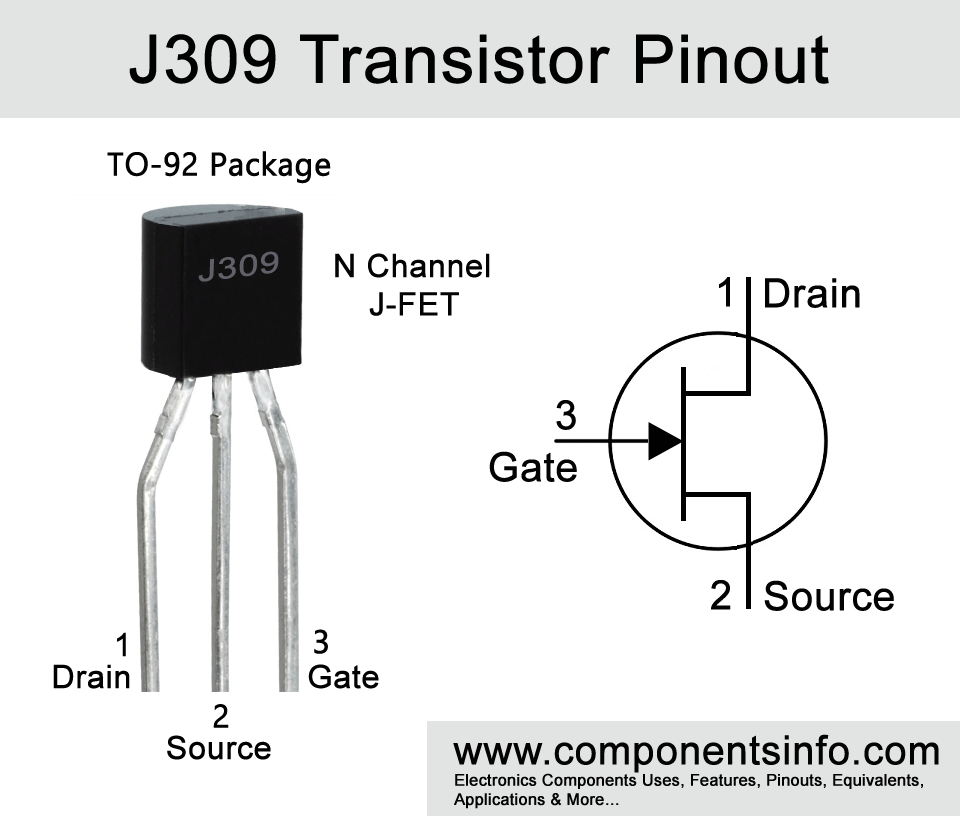
J309 JFET Pinout, Equivalents, Specs, Features, Benefits and Other Information
J309 is an N Channel JFET transistor available in TO-92 and other packages. The transistor is primarily designed for VHF and UHF amplification purposes and contains many features and benefits which we are going to discuss here. The post contains J309 JFET pinout, equivalents, specs, features, benefits of using this transistor and other useful information about this JFET.
Features / Technical Specifications:
- Package Type: TO-92, SOT-23 and TO-52
- Transistor Type: N Channel Depletion
- Max Gate To Drain Voltage Should Be: –25V
- Max Gate To Source Voltage Should Be: –25V
- Max Gate Current is: 10mA
- Minimum to Maximum Gate to Source Cuttoff Voltage : -1.0 to -4.0V
- Max Drain Power Dissipation is: 350mW
- Low Noise Upto 2.7dB Typical Noise Figure
- Max Storage & Operating temperature Should Be: -55 to +150 Centigrade
Replacement and Equivalent:
L310, U310, U309, 2SK125-4
J309 JFET Explained / Description:
J309 is an another transistor of J3xx series in this series there are also other transistor which are j308 and J310. It is an N channel depletion JFET available in TO-92 package with most of the manufacturers but some manufacturers also make it in SOT-23 and TO-52 package.
The main use for which this transistor is designed is in VHF and UHF applications and there are also many features and benefits of using this transistor or its series in your VHF and UHF applications.
First we will discuss about some features of the transistor.
High Sensitivity:
Sensitivity is one of the important factor in RF applications and transistors with high sensitivity are the main component of any RF application because it amplifies the low level signal to high level which is one of the main requirement of any RF design.
Low Noise:
Low noise is also a very important factor. Because most of the time in electronics there is noise with the signal and when we amplify it, the noise also amplifies with it. Hence a transistor with low noise characteristics cuts these extra noises in the signal to a good level and provides a low noise amplified signal at the output.
High gain:
The transistor also contains high gain feature. High gain means it will increase the power of the signal.
Low Distortion:
It also has very low distortion characteristics, the distortion changes the original signal so the low distortion feature ensures original signal at the output.
Above we have discussed some important features of the transistor, now we will discuss the benefits of using J309 in your design.
Benefits of using J309 JFET:
There are many benefits of using this transistor first of all it has very unique features which makes it a good JFET for UHF and VHF applications. Other benefits are “wideband high gain” means the transistor can provide high gain amplification over a wide frequency scale from 105MHz to 450MHz. It has “high quality of amplification” means it amplifies the signal with very high quality by removing noise and provide low nosie, amplified and high gain signal at the ouput. It also has “high low level signal amplification capability” means it is capable to amplify very low level or very small signal. Moreover it also a high speed switching transistor.
Where and How to Use:
As mentioned it is designed for VHF and UHF frequency regions therefore it can be used in wide variety of RF applications.
Applications:
Oscillators
Mixers
VHF amplifiers
UHF amplifiers
Variety of RF applications
Signal amplification
Safe Operating Guidelines / Absolute Maximum Ratings:
Follow the below guidelines to ensure that the transistor in your design or circuit performs well and lasts a long time.
- First of all do no use the transistor to its absolute maximum ratings and always stay 20% below.
- The max gate current is 10mA so do not add more than 8mA load.
- The max gate to source voltage is 25V so do not drive load of more than 20V.
- Always store or operate the transistor at temperature above -55°C and below +150 °C.
Datasheet:
To download the datasheet just copy and paste the below link into your browser.
https://cdn.datasheetspdf.com/pdf-down/J/3/0/J309_ONSemiconductor.pdf