B892 Transistor Pinout, Equivalent, Features, Applications and Other Important Details
2SB892 is a PNP transistor available in TO-92L package. The transistor is designed to be used in large current switching applications under 2A. In this article we will understand B892 transistor pinout, equivalent, features, applications and other important details of this transistor.
Understanding the B892 Transistor:
As discussed 2SB892 is a PNP transistor designed for high current switching. Same as other PNP transistors, it has three pins and each pin is connected to a semiconductor layer inside the transistor, the arrangement of these semiconductor layers are as P-type/N-type/P-type.
The first (Emitter) pin of the transistor is connected to the P-type layer, this layer is heavily doped means it contains a large number of electrons which are ready to flow. At the middle there is a Base and N-type layer which is lightly doped and it is a thin layer. Through Base we can control the flow of current from Emitter to the Collector. The next is the collector layer which is a P-type, this layer has a different work then the first Emitter (P-type), it collects the electrons coming from the Emitter through the Base.
Looking at the ratings of the transistor, the collector-emitter voltage is 50V, this means you can connect any load with the transistor upto 50A. The collector current is 2A which means you can drive upto 2A loads with this transistor. The collector power dissipation of the transistor is 1W which allows the transistor to be used in which makes it suitable for low to moderate power applications. The transition frequency of the transistor is 150MHz which means this transistor can be used in high frequency switching and RF applications around 150MHz. The operating and storage temperature range is from -55°C to +150°C, these are the maximum temperature limits of the transistor and going below or above these limits can damage the transistor.
Moreover, the DC current gain values of the transistor are also very impressive which ranges from 100 to 560 are. The transistor is available in 4 different versions according to its DC current gain and can be determined with the help of the alphabet written below the part number. Here are the details to understand the hFE according to each alphabet:
“R” means 100 to 200 hFE, “S” means = 140 to 280 hFE, “T” means = 200 to 400 hFE and “U” means = 280 to 560 hFE
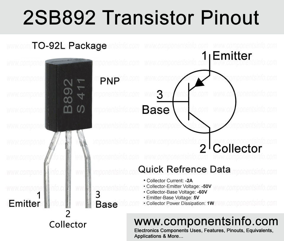
Pin Configuration:
The pin configuration of the transistor are as follows:
- Pin1 (Emitter): As it is a PNP transistor the emitter pin is connected to the positive rail of the circuit.
- Pin2 (Collector): The load is derived through the collector pin. The current enters in the transistor through the emitter and flows to the collector.
- Pin3 (Base): As said above the current flow from the emitter to collector and this current flow is controlled by the base.
Key Features of the Transistor:
- Package Type: TO-92L
- Transistor Type: PNP
- Max Collector Current(IC): -2A
- Max Collector-Emitter Voltage (VCEO): -50V
- Max Collector-Base Voltage (VCBO): -60V
- Max Emitter-Base Voltage (VEBO): -6V
- Max Collector Power Dissipation (PD): 1W
- Current Gain Bandwidth Product(fT): 150MHz
- DC Current Gain is (hFE): 100 to 560
- Max Storage & Operating temperature: -55 to +150 Centigrade
NPN Complimentary
2SD1207
Replacement & Equivalent
2SB1256, 2SB1229, 2SB1318
Advantages & Disadvantages of Using B892:
Here we are pointing advantages and disadvantages of choosing 2SB892 for your circuit or applications.
Advantages:
Low Saturation Voltage:
The low saturation voltage or VCE(sat) improve the transistor’s efficiency and reduces power loss in switching circuits.
High Current Capability:
The maximum collector current is 2A and pulse current is 4A which makes it ideal to drive high an medium loads.
Wide DC Gain Range:
The transistor has quite good DC current gain range that is from 100 to 560 which allows flexibility when designing a circuit.
Good Frequency Response:
The transition frequency of upto150MHz provides fast switching speed and also make the transistor suitable for RF applications around 150MHz.
Disadvantages:
Not Suitable for Very High Voltage Applications:
With collector-emitter voltage (VCEO) of 50V, this transistor cannot be used for high voltage applications.
Moderate Power Dissipation:
The transistor’s collector dissipation is only 1W, which makes the transistor unsuitable for high power applications.
Not Suitable for Amplifier Applications:
This transistor is mainly designed for only switching applications therefore it is not ideal for linear amplifier applications.
Only 2A Collector Current:
With 2A collector current this transistor can only drive low to medium loads.
B892 Applications:
Automotive Electronics
Power Supply Circuits
Lamp Driver Circuits
Relay Driver Circuits
Motor Driver Circuits
Switching Regulators
General Purpose Switching Applications
Conclusion:
2SB892 is a TO-92L Package PNP transistor designed to be used in large current switching applications. The maximum collector current of the transistor is 2A and the maximum load voltage is 50V, the max pulse collector current is -4A, collector power dissipation is 1W, DC Current gain is from 100 to 560 and transition frequency is 150MHz.
As discussed the transistor is good for switching applications but not ideal for linear amplifier applications. The maximum collector current of 2A is good for driving low to medium loads but cannot be used for high current loads above than 2A. Moreover the maximum VCEO voltage is only 50V this also limits the transistor to be used in very high voltage applications.
But if you are looking for a PNP transistor to use as a switch or driver for your small to medium power applications then 2SB892 might be a good option.
Datasheet:
To download the datasheet just copy and paste the below link in your browser.
https://www.alldatasheet.com/datasheet-pdf/view/38800/SANYO/2SB892.html