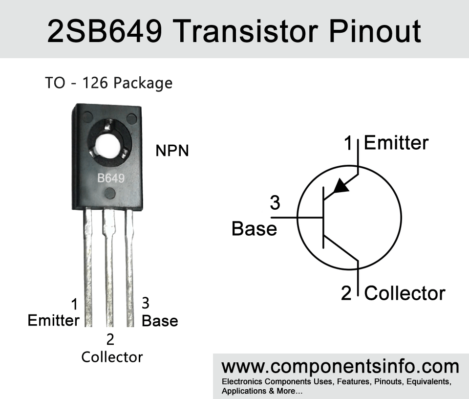
B649 Transistor Pinout, Features, Equivalents, Applications and Other Details.
B649 or 2SB649 is a PNP complimentary of the previously discussed high 2SD669. So if you are looking for a high voltage PNP transistor with upto 1.5A load driving capacity then this transistor can be a good choice. This post describes all the important information such as B649 transistor pinout, features, equivalents, applications and other details.
Features / Technical Specifications:
- Package Type: TO-126
- Transistor Type: PNP
- Max Collector Current(IC): -1.5A
- Max Collector-Emitter Voltage (VCE): -120V
- Max Collector-Base Voltage (VCE): -180V
- Max Emitter-Base Voltage (VBE): -5V
- Max Power Dissipation (Pc): 1W
- Max Transition Frequency (fT): 140 MHz
- Minimum & Maximum DC Current Gain (hFE): 60 to 320
- Max Storage, Operating & Junction temperature range: -55 to +150 Centigrade
PNP Complementary:
PNP complimentary of 2SD669 is 2SB649
Replacement and Equivalent:
2SB1419, 2SB649A, 2SB649B, 2SB649C, 2SB1347
2SB649 Transistor Explained / Description:
2SB649 is a high voltage PNP transistor designed to use as power amplifier in low frequency applications. Moreover the transistor’s collector to emitter voltage is upto -120V which makes it ideal to use in many high voltage applications. Looking at the other maximum ratings of the transistor the collector to base voltage is -180V, emitter to base voltage is -5V, collector current is -1.5A, peak collector current is -3A and collector power dissipation is 1W.
The electrical characteristics of the transistor are collector to emitter saturation voltage -1V, collector output capacitance is 27pF, transition frequency is 140MHz and DC current gain is 60 to 320.
The transistor is available in three different versions according to its hFE values and can be determined with the help of the alphabet written after the part number. If the letter is “B” then its hFE will be 60-120, if “C” then it will be 200-200, and if “D” then its hFE will be 160-320.
Where We Can Use it & How to Use:
D649 can be used in variety of L-F power amplifiers. But it can also be used in other applications like general purpose uses, RF circuits, switching, power supply, voltage amplifiers etc.
Applications:
Voltage amplifiers
Power Supplies
Radio and RF
General purpose
Power supply regulation
Safe Operating Guidelines:
Before operating this device it is important to understand what are the safe operating limits of the transistor. The max ratings of the transistor shown above are the maximum limits on which the transistor can last survive so it is always important to stay at least 20% below from these ratings.
- The max collector to emitter voltage is -120V so you should not drive load of more than -96V.
- The max collector current is -1.5A, therefore the derived load should be under -1.2A.
- Max emitter base voltage should not be more than -5V.
- Max power dissipation should not be more than 1W.
- A suitable heatsink is important to use.
- The storage and operating temperature of the transistor should be between -55°C to +150 °C.
.
Datasheet:
To download the datasheet just copy and paste the below link in your browser.
https://z3d9b7u8.stackpathcdn.com/pdf-down/2/S/D/2SD669A_HitachiSemiconductor.pdf