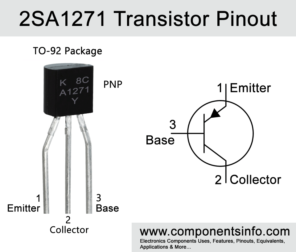
A1271 Transistor Pinout, Features, Equivalent, Applications, Safe Using Guidelines and More
A1271 or full part number 2SA1271 is a PNP transistor available in TO-92 package. This transistor can be used in variety of applications. In this post we are going to discover A1271 transistor pinout, features, equivalent, applications, safe using guidelines and other important info of this device.
Features / Technical Specifications
- Package Type: TO-92
- Transistor Type: PNP
- Max Collector Current (IC): -800mA
- Max Collector-Emitter Voltage (VCEO): -30V
- Max Collector-Base Voltage (VCBO): -35V
- Max Emitter-Base Voltage (VEBO): -5V
- Collector Power Dissipation (PC): 600 mW
- DC Current Gain (hFE): 25 to 240
- Max Storage, Operating & Junction temperature range: -55 to +150 Centigrade
NPN Complementary
NPN Complementary of 2SA1271 is 2SC3203
Replacement and Equivalent
2SB985, 2SB740, 2SA966, BC640‑16, BC327‑025, 2SB978, 2SB892, 2SB1298, 2SB1212, 2SB1059, 2SB1041, 2SA1534A
C3203 Transistor Explained / Description
If you are searching for a TO-92 transistor with good collector current that you can use in different general purpose applications then A1270 can be a good choice. The transistor is actually designed for general switching and low frequency power amplifiers but due to its good features and characteristics it can also be used in wide variety of other applications such as audio preamplifications, RF applications etc.
When looking at the maximum limits of the transistor (Absolute maximum ratings), the maximum collector-emitter voltage (VCEO) is -30V, max collector-current (IC) is -800mA, max collector-base voltage (VCBO) -35V, max emitter-base voltage is -5V and max collector power dissipation (PC) is 600mW.
Some electrical characteristics of the transistor are transition frequency of 120MHz, DC current gain is from 100 to 320, collector emitter saturation voltage is -0.7V and output capacitance is 19pF typical.
The transistor is available in two different versions according to its DC current gain or HFE and you can differentiate the two by the alphabet written after the part number. If that alphabet is “O” then the HFE of that transistor will be 100 to 200 and if that alphabet is “Y” then the HFE will be 160-320.
Where We Can Use it & How to Use
The transistor is designed to use for general purpose switching and in audio frequency power amplifiers but it is not limited to these uses and can be used in wide variety of other applications. Using procedure is same as we use other BJT transistor.
Applications
Switching circuits
Audio amplifier circuits
Audio preamplifiers
Darlington pairs
RF circuits around 120MHz
Driver Circuits
Communication circuits
And variety of other general purpose applications.
Safe Operating Guidelines
To safely operate the transistor it is essential to not use the transistor to its absolute maximum ratings or max limits. The transistor must be operated 20% below from its absolute maximum ratings. This technique will provide less load on the transistor which makes it perform good and long term in an electronic circuit. So the maximum collector current is -800mA so we should not drive load of more than 640mA. The maximum collector-emitter voltage is -30V therefore do not drive a load of more than -24V, the maxi power dissipation should not be more than 500mW and the storage or operating temperature of the transistor must be between -55°C to +150°C.
Datasheet
To Download the datasheet just copy and paste the below link in your browser.
https://z3d9b7u8.stackpathcdn.com/pdf-down/2/S/A/2SA1271_KEC.pdf