J113 Transistor Pinout, Equivalent, Applications, Features and More
This post contains all the important information about J113 transistor pinout, equivalent, applications, features and where and how to use this JFET.
Features / Technical Specifications:
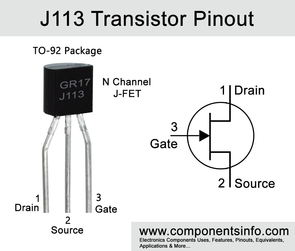
- Package Type: TO-92, SOT-23
- Transistor Type: N Channel JFET (Symmetrical)
- Maximum Drain to Gate Voltage: 35V
- Maximum Reverse Gate to Source Voltage: –35V
- Maximum Continues Gate Current: 50mA
- Maximum Gate to Source Cutoff Voltage : –5 to –3V
- Maximum Power Dissipation: 625mW
- Max Storage & Operating temperature Should Be: -55 to +150 °C
- Drain and source are exchangeable.
Replacement and Equivalent:
J111, J112
Nearest Possible Equivalents:
2N4416, J201, j202, j203, NTE312, NTE458, 2N4340, 2N4341. These are the nearest possible equivalents of J113 some of the devices in these equivalent transistors may not have symmetrical feature.
J113 Transistor Explained / Description:
J113 is an N Channel silicon FET or field effect transistor of J11x series. Other transistors in this series are J111 and J112. The transistors are available in TO-92 and SOT-23 packages.
They are primarily designed to be used in choppers, sample and hold applications, current limiting applications, switching applications, commentators etc.
Benefits of using these transistors are high switching speed, better response to frequency, good accuracy, low cost, low insertion loss etc.
The maximum gate to source voltage of the transistor is 35V, max reverse gate to source voltage is -35, maximum continues gate current is 50mA and maximum power dissipation is 625mW. It is a Symmetrical transistor which means the source and drain leads can be swapped.
Where We Can Use it & How to Use:
J113 can be used in wide variety of applications; it can be used in current limiting circuits, chopper circuits and verity of analog switching circuits. Other than that it can also be used in high gain amplifier applications to increase gain of any type of electronic signal.
Applications:
Low level signal amplification
Audio preamplifiers
High gain amplifiers
Sensor & detector circuits
Current limiting circuits
Analog switching circuits
Safe Operating Guidelines / Absolute Maximum Ratings:
To safely operate J113 JFET or any other transistor it is recommended to always operate it under its absolute maximum ratings. Operating the transistor to its absolute maximum ratings may affect it and reduce its performance. Therefore always stay 20% below from the absolute maximum ratings.
The maximum gate current is 50mA therefore do not drive load of more than 40mA, the maximum drain to gate voltage is 35V therefore do not drive load of more than 28V and always store or operate the device at temperature above -55°C and below +150 °C.
Datasheet:
To Download the datasheet just copy and paste the below link in your browser.
https://cdn.datasheetspdf.com/pdf-down/J/1/1/J113_FairchildSemiconductor.pdf