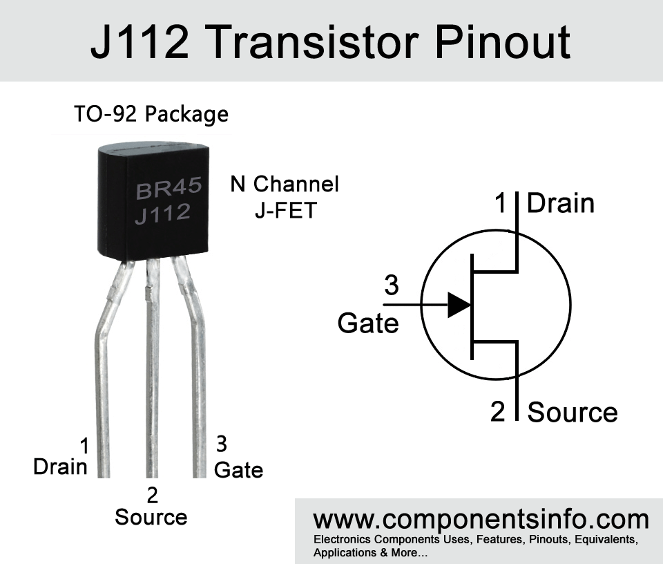
J112 Transistor Pinout, Equivalents, Applications and Other Details
J112 is another transistor of J11x series. In this post we are going to discuss about J112 transistor pinout, equivalents, applications and other details about this JFET.
Features / Technical Specifications:
- Package Type: TO-92, SOT-23
- Transistor Type: N Channel JFET (Symmetrical)
- Maximum Drain to Gate Voltage: 35V
- Maximum Reverse Gate to Source Voltage: –35V
- Maximum Continues Gate Current: 50mA
- Maximum Gate to Source Cutoff Voltage : –5 to –3V
- Maximum Power Dissipation: 625mW
- Max Storage & Operating temperature Should Be: -55 to +150 °C
- Drain and source are exchangeable.
Replacement and Equivalent:
J111, J113
Nearest Possible Equivalents:
2N4416, J201, j202, j203, NTE312, NTE458, 2N4340, 2N4341. Here are some of the nearest possible substitute or equivalents of J112 but they may not have symmetrical feature.
J112 Transistor Explained / Description:
J112 is a high-performance N channel silicon FET or field effect transistor of the J11x series. Other transistors in this rage include JS111 and 112 which have similar uses but differing specs to suit particular requirements. But the primary applications for which these transistors are designed for are sample and hold applications, choppers, analog switching applications, commentators, current limiting etc.
There are also some benefits of using these transistors on particular applications basis such as these transistors are suitable for high speed switching, they provide better response to frequency, they have good accuracy, provide low insertion loss, they also have symmetrical feature which means the source and drain can be swapped other than these benefits they are also very low cost.
Regarding to the specs of the transistor their maximum gate to source voltage is -35, maximum power dissipation is 625mW, and maximum continuous gate current is 50mA. These transistors are available in two different packages which are TO-92 and also in small SOT-23 package.
Where We Can Use it & How to Use:
As mentioned above the primary application of J112 are analog switching, chopper circuits, current limiting applications etc. But it can also be used in variety of other applications such as high gain amplification circuitry and amplification of any type of low gain electronic signal.
Applications:
Audio preamplifiers applications
High gain amplifiers circuits
Low level signal amplification applications
Sensor & detector applications
Current limiting circuits
Analog switching applications
Safe Operating Guidelines / Absolute Maximum Ratings:
Before using a transistor in your design or circuit, it is important to be aware of its safety guidelines and absolute maximum rating. It is also not recommended by their manufacturers to use any component at its maximum rating. We therefore recommend that the transistor be used at least 20% below its absolute maximum rating. Therefore the same procedure applies to J112 JFET, the maximum gate current is 50mA so the derived load should be less than 40mA, the maximum drain-to-gate voltage is 35V so the derived load should be less than 28V and transistor should be stored or operated at room temperature above -55°C and below +150 °C.
Datasheet:
To Download the datasheet just copy and paste the below link in your browser.
https://cdn.datasheetspdf.com/pdf-down/J/1/1/J112_FairchildSemiconductor.pdf