J111 Transistor Pinout, Description, Equivalents, Features, Applications and More
J111 is a versatile field effect transistor with many features and benefits. In this post we are going to discuss J111 transistor pinout, description, equivalents, features, applications, benefits of using these transistors in your design or circuits and other details.
Features / Technical Specifications:
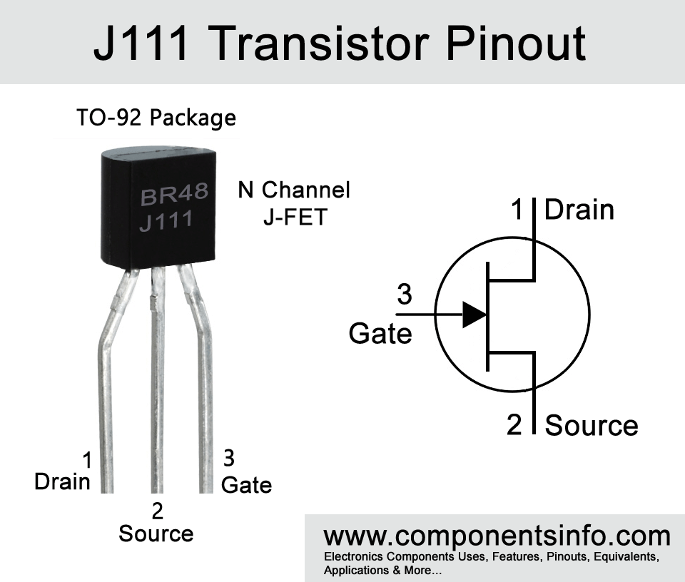
- Package Type: TO-92, SOT-23
- Transistor Type: N Channel JFET (Symmetrical)
- Maximum Drain to Gate Voltage: 35V
- Maximum Reverse Gate to Source Voltage: –35V
- Maximum Continues Gate Current: 50mA
- Maximum Gate to Source Cutoff Voltage : –5 to –3V
- Maximum Power Dissipation: 625mW
- Max Storage & Operating temperature Should Be: -55 to +150 °C
- Drain and source are exchangeable.
Replacement and Equivalent:
J112, J113
Nearest Possible Equivalents
2N4416, J201, j202, j203, NTE312, NTE458, 2N4340, 2N4341 are the nearest possible substitute of J112 but they may not have symmetrical feature.
J112 Transistor Explained / Description:
J111 is an N channel silicon field effect transistor available in TO-92 and SOT-23 packages. J111 is a transistor from J11x series, this series also contains J112 and J113 transistors. All the transistors in this series are primarily built to use for analog switching applications, current limiting, choppers, commentators and sample and hold applications.
There are also many benefits of using these transistors in your design such as they provide better response to frequency, they have good accuracy, low insertion loss and they are also low cost. Moreover the transistor also has low noise feature which means it can be used in applications where the user also has low noise requirements. The transistor also has Symmetrical features which means the drain and source of the transistor are interchangeable.
When we look at the specs of the transistor the maximum drain to gate voltage is 35V, maximum continuous gate current is 50mA, maximum reverse gate to source voltage is -35V, max gate to source cutoff voltage is -0.5 to 3V and the max power dissipation is 625mW.
Where We Can Use it & How to Use:
As mentioned above that J111 FET or field effect transistor is primarily designed for current limiting, analog switching, choppers, commentators and sample and hold applications but J111 transistor is a versatile device that can be used in a variety of applications. If you need a fast switching transistor with low leakage and low capacitance, then the J111 is a good choice.
Applications:
High speed switching
Audio preamplifiers
High gain amplifiers
Low level signal amplification applications
Sensor & detector circuits
Current limiting
Analog switching applications
Safe Operating Guidelines / Absolute Maximum Ratings:
It is always recommended to check absolute maximum ratings of the transistor before using in your design or circuit and we also suggest to not use a component on its absolute maximum ratings and always stay atlest 20% below from the absolute max ratings. Therefore same applies to J111 transistor. The maximum drain to gate voltage is 35V therefore do not drive load of more than 28V. The maximum continuous gate current is 50mA so do not drive load of more than 40mA and always store or operate the transistor at temperature above -55°C and below +150 °C.
Datasheet:
To Download the datasheet just copy and paste the below link in your browser.
https://cdn.datasheetspdf.com/pdf-down/J/1/1/J111_FairchildSemiconductor.pdf