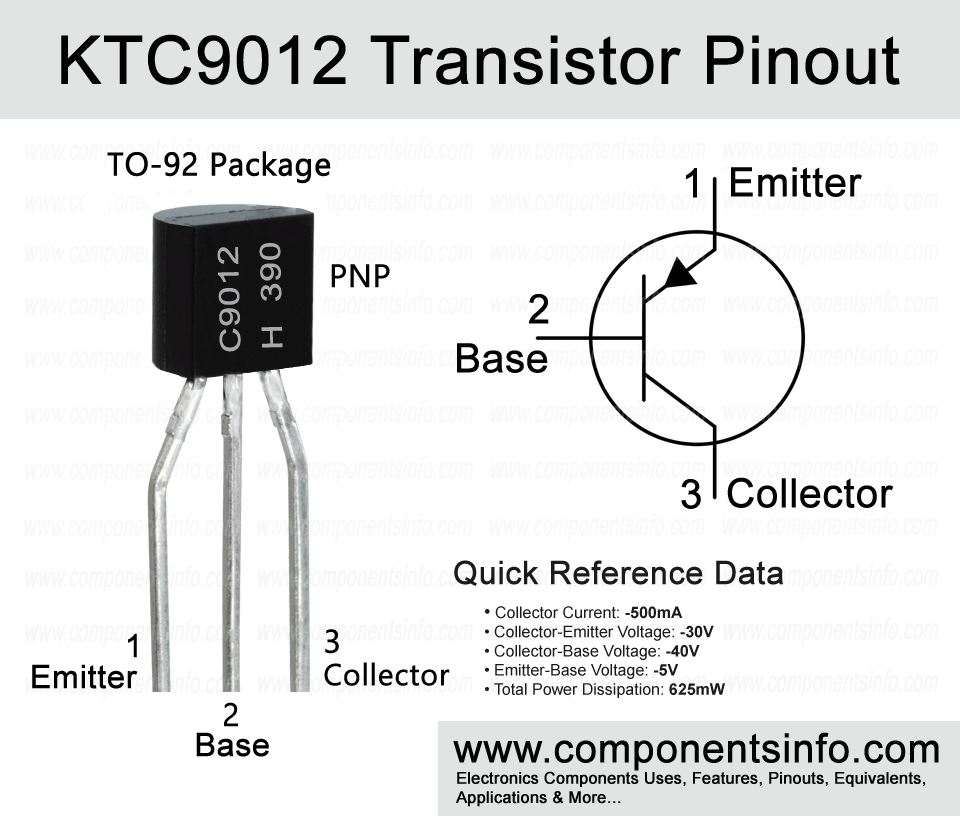
C9012 Transistor Pinout, Equivalents, Features, Applications and More
C9012 is an NPN transistor available in TO-92 package. Its full part number is KTC9012. It is designed to be used in switching and general purpose applications. This post contains information about C9012 transistor pinout, equivalents, features, applications and other details about the transistor.
Absolute Maximum Ratings:
- Package Type: TO-92
- Transistor Type: PNP
- Max Collector Current(IC): -500mA
- Max Collector-Emitter Voltage (VCE): -30V
- Max Collector-Base Voltage (VCB): -40V
- Max Emitter-Base Voltage (VEBO): -5V
- Max Collector Dissipation (Pc): 625 miliWatt
- Max Transition Frequency (fT): 150 MHz
- Minimum & Maximum DC Current Gain (hFE): 64 – 246
- Max Storage & Operating temperature Should Be: -55 to +150 Centigrade
PNP Complementary:
PNP Complementary of KTC9012 is KTC9013
Replacement & Equivalent
KTC9015, BC337‑040, KTC3202, KTC3205, KTN2222A, P2N2222A, KTC1006, 2SC1735, 2SD790, 2SC3328, ZTX455, ZTX653, ZTX651, ZTX851, ZTX450, NTE382, BC537, MPSW05, MPS6602, MPSW01, SK9137, SK3250, SK3854, KSP05.
KTC9012 Transistor Explained / Description:
Previously we have discussed C9013 transistor which is a NPN complimentary of C9012 and today we are going to discuss about C9012 PNP transistor. This PNP complimentary is also very interesting and having many good features such as good collector current, good transition frequency, good collector power dissipation and availability of its NPN complimentary.
Looking at the absolute maximum ratings of the transistor the collector current is -500mA, collector emitter voltage is -30V, collector-base voltage is -40V, emitter-base voltage is -5V, emitter current is 500mA, collector power dissipation is 625mW, junction temperature is 150°C and storage temperature is -55°C to 150°C.
The transistor is available in 6 different variations according to DC current gain and can be identified with the help of a letter / alphabet written after its part number. He are the details of DC current gain meaning of each letter/alphabet.
D= 64-91
E= 78-112
F=96-135
G=118-166
H=144-202
I= 176-246
C9012 is designed for switching and general purpose applications such as amplifiers, switching, RF applications and more. The detailed list can be found under the Applications heading below.
How to Use This Transistor:
It is a BJT transistor therefore the using procedure is same as we use any other BJT by connecting its emitter pin with the positive rail of the circuit, applying signal to its base pin, signals from which you want to amplify (in amplifier circuit) or from which you want to control the output (in a switch circuit) load.
Applications:
Audio Amplifiers
Sensor Circuits
Signal Amplification
RF Circuits
Darlington Pairs
Audio Preamplifiers
Switching loads under 100mA
And more…
Safe Operating Guidelines:
For safe operation of the transistor do not drive it to its absolute maximum ratings and always stay at leat 20% below. Always check its pin layout before use and make sure the temperature should be between -55°C to 150°C.
Datasheet:
To download the datasheet just copy and paste the below link in your browser.
https://www.alldatasheet.com/datasheet-pdf/view/69891/KEC/KTC9012.html