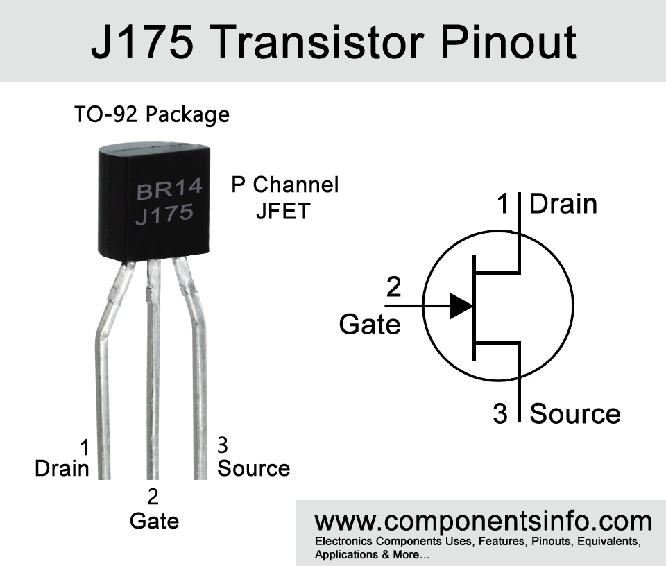
J175 JFET Pinout, Equivalent, Applications, Features and Other Related Details
J175 is a P Channel JFET available in TO-92 and SOT-23 packages. This article covers a detailed overview of J175 JFET pinout, equivalent, applications, features and other related details.
Features / Technical Specifications:
- Package Type: TO-92 & SOT-23
- Transistor Type: P Channel JFET
- Maximum Drain to Gate Voltage: -30V
- Max Gate to Source Voltage: 30V
- Max FWD Gate Current: 50mA
- Zero to Gate Voltage Drain Current: -7.0mA to -60mA
- Maximum Device Dissipation: 350mW
- Drain to Source On Resistance: 125Ω
- Max Storage & Operating temperature Should Be: -55°C to +150 °C
Replacement and Equivalent:
J176, J177
J175 Transistors Explained / Description:
J175 is a P Channel JFET or field effect transistor available in TO-92 and SOT-23 packages. This device is mainly designed to use in chopper stabilized amplifiers it is an application that reduces drift and noise in an electronic signal. What these circuits do is that they cut a small DC electronic signal into many AC signal and then amplify each signal and in the end combines these AC amplified signal and then convert them into a DC signal again. These types of circuits are used in devices which require stability and accuracy for example measurement and medical instruments etc.
Another application of this transistor is a sample and hold circuit. This circuit is useful in electronics where measurement accuracy is required. The devices in which sample and hold circuits are used are scientific instruments, Medical devices, communication (to convert an analog signal to a digital signal), automotive systems (In Engine Management Systems), and also in Robotics (To hold sensor data for measurement and control).
It is a versatile transistor and not limited to these applications only and it can also be used in variety of other applications.
Looking at the specs of the transistor the maximum drain to gate voltage is -30V, the max gate to source voltage is 30V, the max fwd gate current is 50mA, zero to gate voltage drain current is -7.0mA to -60mA, the maximum device dissipation is 350mW and drain to source on-resistance is 125 Ohms.
Some of the main features of the transistor are:
Low ON-Resistance:
The low ON resistance is the resistance between drain and source of the transistor when the transistor is fully ON mode. When any transistor has low ON resistance it has low voltage drop between its drain to source which is beneficial.
Fast Switching:
As the heading suggests, it is a fast switching transistor and has only 25 nanoseconds turn on time due to which it can be useful in circuits that require fast switching speed.
Low Leakage:
It has very low leakage current which is only 10 picoamps, the low leakage current is important in devices that require high accuracy when the transistor is switched off.
Low capacitance:
The low capacitance is also an important factor in overall transistor performance, the low capacitance in a transistor improves its performance and speed.
Low Insertion Loss:
The low insertion loss feature maintains the signal strength when a signal is passing through the transistor.
The other features and benefits are low error voltage, good frequency response, and good overall accuracy.
Where We Can Use it & How to Use:
As mentioned above J175 is a JFET designed to use in chopper stabilized amplifiers, sample and hold circuits etc. The detailed list of its applications can be found under the applications heading below. To use the transistor you have to check the operating parameters and biasing and follow other operating conditions mentioned in the datasheet.
Applications:
Voltage Regulators
Oscillators
RF Amplifiers
Sample and Hold
Switching Circuits
Instrumental Amplifier
Signal Modulation & Demodulation
Low Noise Applications
Low Level Signal Amplification
Automotive Applications
Safe Operating Guidelines / Absolute Maximum Ratings:
To safely operate the transistor and get long term performance it is suggested to not drive it to its absolute maximum ratings and always stay 20% below from its absolute maximum ratings. It is also important to use it in the suggested temperate range which is from -55°C to +150 °C.
Datasheet:
To Download the datasheet just copy and paste the below link in your browser.
https://z3d9b7u8.stackpathcdn.com/pdf-down/J/1/7/J175_FairchildSemiconductor.pdf