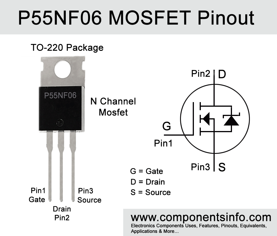
P55NF06 MOSFET Pinout, Features, Equivalents, Benefits, Applications and Other Info
This post contains P55NF06 MOSFET pinout, features, equivalents, benefits, applications and other useful and important information about this transistor.
Features / Technical Specifications:
- Package Type: TO-220
- Transistor Type: N Channel
- Max Voltage Applied From Drain to Source: 60V
- Max Gate to Source Voltage Should Be: ±20V
- Max Continues Drain Current is: 50A
- Max Pulsed Drain Current is: 200A
- Max Power Dissipation is: 30W (Some manufacturers also make it around 100W)
- Max Drain to Source Resistance in ON State (RDS on): 0.018Ω
- Max Storage & Operating temperature Should Be: -55 to +150 Centigrade
Replacement and Equivalent:
IRF4410A, BR80N75, BR75N75, 110N10, 80N06, 75N06, 65N06, 50N06, BUK7509‑75A, CS4145, IRF3256, IRFB7740
P55NF06 MOSFET Explained / Description:
P55NF06 is an N Channel MOSFET that is manufactured in different packages the most common package is TO-220 package. It is also searched with STP55NF06, STB55NF06, STP55NF06FP and all are same.
The transistor is primarily designed for power supplies, networking DC to DC power systems, and automobile applications but we can also use it in variety of different applications according to its specs. Moreover, it has many features and benefits which are mentioned below.
Low RDS(on)
The maximum RDS(on) of the transistor is only 0.018 Ω. The low RDS(on) means less resistance when the transistor is ON or driving load and also generates less heat during the operation.
100% Avalanche Tested
It is 100% avalanche tested which means that the device will perform stably in conditions when its drain to source voltage is above from its mentioned drain to source ratings.
Fast Switching Speed
The MOSFET also features high switching speed which is beneficial for applications that require very fast switching of loads such as UPS circuits.
Other features are Improved dv/dt capability, ultra low gate charge, etc.
Where We Can Use It & How to Use:
As mentioned the MOSFET is primarily designed for power supplies, networking DC to DC power systems and automobile applications but can also be used in a variety of general applications which fall under its ratings such as motor controllers, audio amplifiers etc.
Applications:
Power Supplies
Solar Chargers
Uninterruptible Power Supplies
Battery Chargers
Battery Management Systems
Audio Amplifiers
Motor Controllers
Inverter Circuits
Safe Operating Guidelines / Absolute Maximum Ratings:
To safely operating the device follow the guidelines below:
- Do not use the transistor to its absolute maximum ratings and always use it 20% below from its max ratings.
- The maximum continuous drain current is 50A therefore do not drive load of more than 40A.
- The maximum drain to source voltage is 60V therefore do not drive load of more than 48V.
- Always use a suitable heatsink with the MOSFET.
- Always store or operate at temperatures above -55 °C and below +150 °C.
Datasheet:
To download the datasheet just copy and paste the below link into your browser.
https://cdn.datasheetspdf.com/pdf-down/S/T/P/STP55NF06_STMicroelectronics.pdf