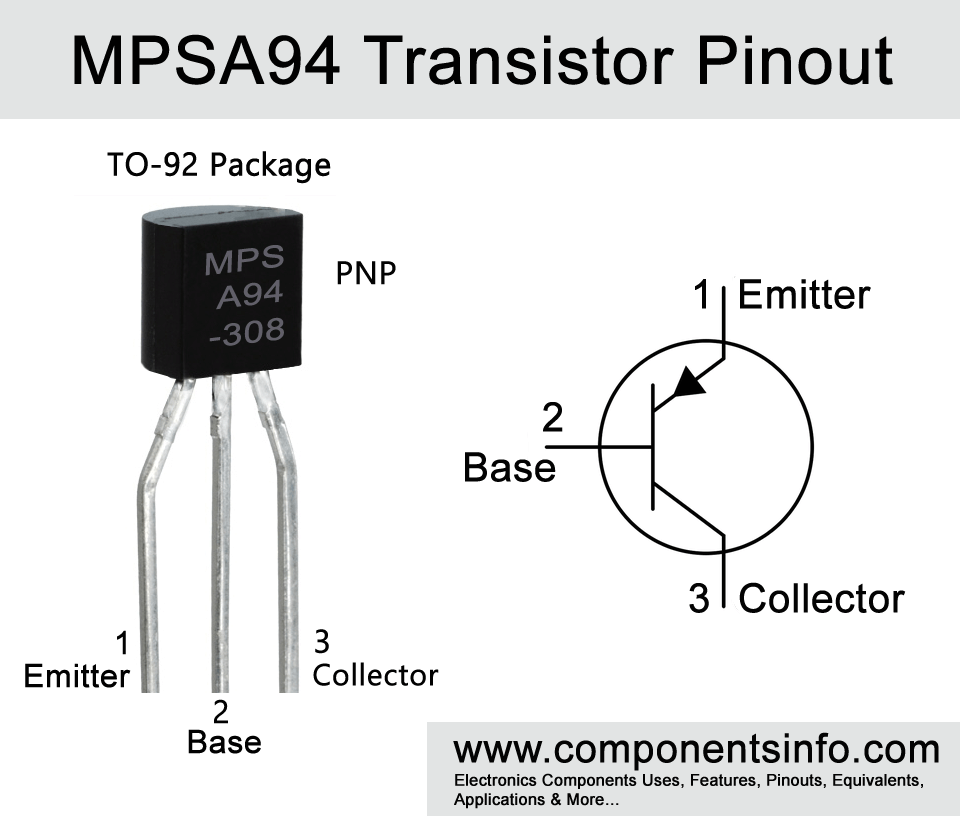
MPSA94 Transistor Pinout, Equivalent, Uses, Features and Other Info
This post contains all the important information about MPSA94 transistor pinout, equivalent, uses, features and other info about the transistor.
Absolute Maximum Ratings:
- Package Type: TO-92
- Transistor Type: NPN Silicon
- Max Collector Current(IC): 300mA
- Max Collector-Emitter Voltage (VCEO): –400V
- Max Collector-Base Voltage (VCBO): –400V
- Max Emitter-Base Voltage (VEBO): –6V
- Total Device Dissipation (Pc): 625mW
- Minimum & Maximum DC Current Gain (hFE): 40 To 200
- Max Storage & Operating temperature: -65 to +150 Centigrade
NPN Complementary:
NPN Complementary of MPSA94 is MPSA44
Replacement and Equivalent:
MPSA94A, MPSA194, KSP94
MPSA94 Transistor Explained / Description:
MPSA94 is a TO-92 package high voltage PNP transistor designed to use in telecommunication applications and applications which demands high voltage but low current transistor.
Absolute maximum ratings of the transistor are collector to base voltage of -400V, collector to emitter voltage of -400V, collector current is -300mA, collector power dissipation is 625mW and operating and storage junction temperature is from -55 °C to +150°C.
The electrical characteristics of the transistor are as follow:
In ON state it has collector to emitter saturation voltage of -0.5V at -1mAdc, DC current gain of 40 to 300. The transistor also has protective measure when it is in Off state. Such as collector cut off current of -100nA and collector to emitter breakdown voltage of -400V.
The thermal resistance, junction to case is 83.3 °C /W, this ratings shows how much the transistor is efficient to dissipation of heat through its case.
Where We Can Use it & How to Use:
As mentioned above this transistor is mainly designed to use in high voltage circuits and telecommunications but it can also be used in many switching and amplifier applications. Using procedure of the transistor is just like any other PNP BJT transistor such as the emitter pin will be connected with the positive supply, the base pin will be connected with the input signal or the signal which you want to amplify or use as a switch but make sure to use a suitable resistor between the signal and the base when using it as a switch. Now third pin that is collector will be connected with positive wire/lead/connection of the load and the other wire/lead/connection of the load will be connected with the negative supply of the circuit.
Applications:
Audio Amplification
Low Voltage Switching
High Voltage Switching
Sensor Circuits
Signal Amplification
Driving Loads under 0.3A
High Voltage Relay Driving
Safe Operating Guidelines:
Always follow these safety guidelines while using the transistor. First of all, make sure that the transistor is not derived to its absolute maximum ratings and always stay 20% below from its max ratings. So to do this, we have to calculate values to get the accurate output. The maximum collector current is -300mA so do not drive load more than -240mA and store or operate the transistor at temperatures between -55°C to 150°C.
Datasheet:
To download the datasheet just copy and paste the below link in your browser.
https://z3d9b7u8.stackpathcdn.com/pdf-down/M/P/S/MPSA94_KEC.pdf