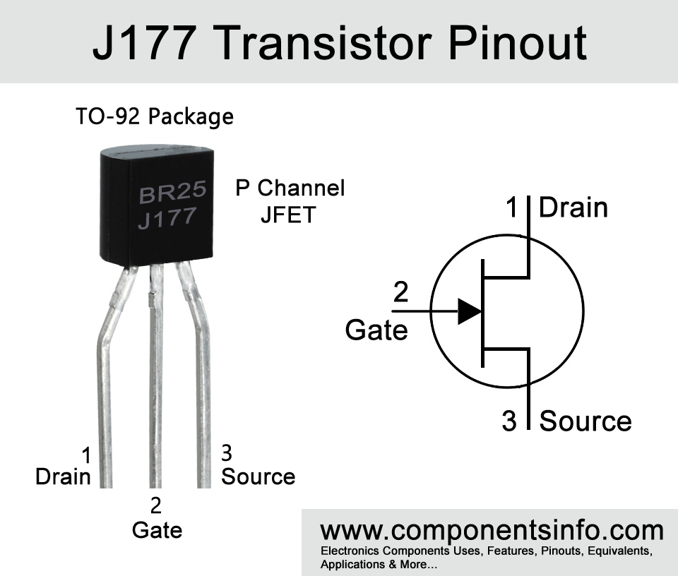
J177 JFET Pinout, Applications, Equivalent, Features and Other Important Details
In this post, we are going to discuss about J177 JFET transistor. The post contains J177 JFET pinout, applications, equivalent, features, and other important details and explanation about the transistor.
Features / Technical Specifications:
- Package Type: TO-92 & SOT-23
- Transistor Type: P Channel JFET
- Maximum Drain to Gate Voltage: -30V
- Max Gate to Source Voltage: 30V
- Max FWD Gate Current: 50mA
- Zero to Gate Voltage Drain Current: -1.5mA to -20mA
- Maximum Device Dissipation: 350mW
- Drain to Source On Resistance: 300Ω
- Max Storage & Operating temperature Should Be: -55°C to +150 °C
Replacement and Equivalent:
J174, J175, J176
J177 Transistors Explained / Description:
J177 is a P Channel JFET (Junction Field Effect Transistor). It is a transistor of a series in which there are three more JFETs and their part numbers are J174, J175, J176. J177 is the last part number of the series. This series of JFETs are designed to use in many applications such as
Chopper Stabilized Amplifier:
Chopper stabilized amplifier is a circuit that is used to reduce the noise and drift in an electronic signal. The circuit does this by cutting a small DC signal into many AC signals and then amplifying each signal separately and in the end, it combines all these amplified AC signals into one DC signal. These types of circuits are very useful in devices that require higher accuracy such as measurement instruments, medical instruments, scientific instruments, etc.
Sample and Hold Circuits:
Another application in which this transistor is designed to use in sample and hold circuits. Sample and hold circuits as the name suggest these circuits are used in electronics to hold a sample of an analog signal of a particular time moment and holds it. The sample and hold circuit contains two stages the first stage is a sample stage which sample an input signal. The second stage is a hold stage which store a sampled voltage for a time period. These types of circuits are used in analog to digital converter circuits, audio processing, etc.
Low Level Analog Switching:
Low level analog switching is an application used for switching small magnitude signals for example in micro or millivolts. Audio circuits are one of a good example of these signals. So what these transistors do is amplify these signals without any loss in the signal and distortion and hence we get an accurate signal at the output. Or in other words, we can say that low level analog switching is important when we are more concerned about the accuracy of the signal at the output some other examples of this are filters, equalizers, etc.
Now looking are the main features of the transistor which make it more reliable and versatile are low on-resistance, fast switching, low leakage, low insertion loss, low capacitance, low error voltage, good frequency response and good overall accuracy.
The absolute maximum ratings of the transistor are max drain to gate voltage is 30V, max gate to source voltage is 30V, zero to gate voltage drain current is -1.5mA to -20mA, max FWD gate current is 50mA, max device dissipation is 350mW and drain to source on-resistance is 300 Ohms.
Where We Can Use it & How to Use:
It can be used in Choppers, Current Limiters, Normally “ON” Switches, etc. The detailed list of its applications can be found under the Applications heading below. The transistor can be used as a switch as well as an amplifier. For using the transistor in your design it is important to check and follow its operating parameters and operating conditions from the datasheet.
Applications:
Sample and Hold
Voltage Regulators
Switching Circuits
RF Amplifiers
Signal Modulation & Demodulation
Low Level Signal Amplification
Oscillators
Low Noise Applications
Automotive Applications
Instrumental Amplifier
Safe Operating Guidelines
To get long term performance with this transistor it is important to always follow the safe operating guidelines before using it in your design or circuit. One of the important point to keep in mind is to not operate any transistor or component to its absolute maximum ratings and always stay at least 20% below from its max ratings. Moreover always store of operate the transistor at temperatures above -55°C and below 150 °C.
Datasheet:
To Download the datasheet just copy and paste the below link in your browser.
https://z3d9b7u8.stackpathcdn.com/pdf-down/J/1/7/J177_FairchildSemiconductor.pdf