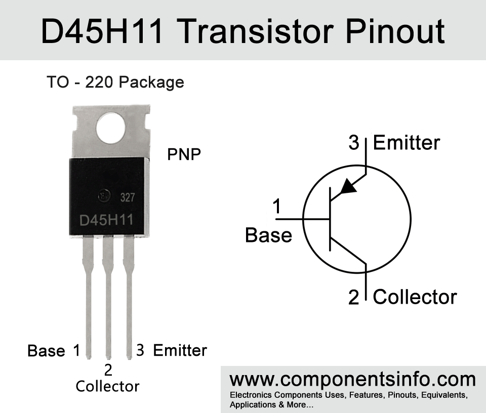
D45H11 Pinout, Features, Explanation, Specs, Applications, and Other Technical Info
D45H11 is a general purpose versatile PNP transistor that can be used in various applications. The post below describes D45H11 pinout, features, explanation, specs, applications, and other technical information.
Features / Technical Specifications:
- Package Type: TO-220
- Transistor Type: PNP
- Max Collector Current(IC): -10A
- Max Collector Current in Pulses (ICP): -20A
- Max Collector-Emitter Voltage (VCE): -80V
- Max Emitter-Base Voltage (VEBO): -5V
- Max Collector Dissipation (Pc): 50 Watt
- Max Transition Frequency (fT): 50 MHz
- Minimum & Maximum DC Current Gain (hFE): 40 – 60
- Max Storage & Operating temperature Should Be: -55 to +150 Centigrade
Replacement and Equivalent
These are the low voltage equivalents of D45H11 and if your load requirement is lower than 80V then you can easily replace them with D45H11. With the part numbers we have also mentioned their collector to emitter voltage so that you can decide which number will better suit your circuit requirements.
D45H1 (VCEO = -30), D45H2 (VCEO = -30), D45H4 (VCEO = -45), D45H5(VCEO = -45), D45H7(VCEO = -60), D45H58(VCEO = -60), D45H10(VCEO = 80).
NPN Complementary
The NPN complimentary of D45H11 is D44H11
D45H11 Transistor Explained / Description:
D45H11 is a PNP version or complementary of D44H11 transistor that we have discussed earlier. It is also a general purpose transistor with many features. For example, it has a low saturation voltage due to which will become activated on very low base voltage. With only 0.2V on its base it can drive load of upto 3A, with 0.4V it can drive load of upto 5A and become fully saturated to drive load of upto 10A at 0.58V. Another feature is its fast switching speed of nano seconds. It has a delay and rise time of 135ns, Storate Time of 500ns, and Fall Time of 100ns.
Looking at the specs of the transistor the maximum collector current is -10A, max pulsed collector current is -20A, emitter to base voltage is -5V, minimum DC current gain is 40 to 60, max transition frequency is 50MHz and max collector dissipation is 50W.
The transistor is designed to use in general purpose switching applications combined with its fantastic characteristics making this transistor capable of being used in variety of general purpose switching and amplification applications of commercial as well as educational electronics.
Where We Can Use it & How to Use
D45H11 can be used for a variety of purposes such as power audio amplification, switching circuit which requires high speed switching, voltage regulation, etc. The detailed list of applications can be found below under the application heading.
Applications
Battery Chargers
Motor Driver Circuits
Power supplies
Automotive Circuits
High Power Audio Amplifiers
Solar Applications
And Much More…
Safe Operating Guidelines / Absolute Maximum Ratings:
Follow the below guidelines to safely operate the transistor to get long term performance.
- To get long term performance it is important to check the absolute maximum ratings of the transistor and design the circuit that drives the transistor atleast 20% below from its absolute maximum ratings. Such as the maximum continuous collector current of the transistor is 10A therefore the driven load should be under 8A. The maximum collector to emitter voltage is 80V therefore the driven load should be under 64V.
- A proper heatsink is also essential to use with the transistor. A suitable heatsink dissipates transistor’s heat to air making the internal circuitry of the transistor under its max heat limits.
- Additionally do not store or operate the transistor at temperatures below -55 °C and above +150 °C.
Datasheet
To Download the datasheet just copy and paste the below link in your browser.
https://z3d9b7u8.stackpathcdn.com/pdf-down/D/4/5/D45H-ONSemiconductor.pdf