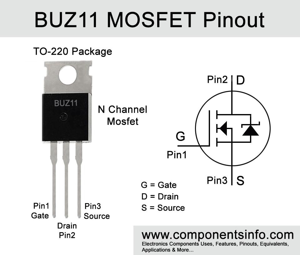
BUZ11 MOSFET Pinout, Explanation, Specs, Equivalents, Features, Applications
BUZ11 is a widely used transistor available in TO-220AB package. In this post we are going to discuss BUZ11 MOSFET pinout, explanation, specs, equivalents, features, applications, and other important information about this device.
Features / Technical Specifications:
- Package Type: TO-220AB
- Transistor Type: N Channel
- Max Voltage Applied From Drain to Source: 50V
- Max Gate to Source Voltage Should Be: ±20V
- Max Continues Drain Current is: 30A
- Max Pulsed Drain Current is: 120A
- Max Power Dissipation is: 75W
- Max Drain to Source Resistance in ON State (RDS on): 0.040Ω
- Max Storage & Operating temperature Should Be: -55 to +150 Centigrade
Replacement and Equivalent:
BUZ11A, BUZ11AL, BUZ11FI, BUZ11S2, IRLZ24N, IRLZ34, IRLZ34N, STP32N06L, STP36N06, MTP30N06EL, RFP23N06LE, STP32N05L, BUK555-60A
BUZ11 Transistor Explained / Description:
BUZ11 is a widely used N Channel MOSFET available in TO-220AB package capable to drive continuous load of up to 30A. It is primarily designed for applications such as high-speed switching, high current switching, switching regulators, DC to AC and DC to DC conversion circuitry, relay driver, high-power audio amplifiers, and motor drivers. But it can also be used in a wide variety of general applications that fall under its ratings.
The MOSFET has many features and benefits such as:
High Load Current and Voltage
The transistor is capable to drive continuous high current load of upto 30A and high voltage load of up to 50V.
Switching Speed of Nano Seconds
The nano speed switching feature makes it ideal for applications in which very high-speed switching is crucial such as in a UPS circuit.
100% Avalanche Tested
The MOSFET is 100% avalanche tested due to which it can withstand and perform stable when its drain to source voltage exceeds from the max limits.
Operated Directly from Integrated Circuits
The transistor is easy to drive and can be directly operated ICs and electronic platforms such as Arduino and Raspberry Pi.
High Input Impedance
The high input impedance decreases the input current and the power dissipation of the MOSFET.
Very Low RDS(on)
The MOSFET has very low drain to source resistance in ON state which ensures less heat dissipation during operation.
The other features are linear transfer capabilities, majority carrier device etc.
The ratings of the MOSFET also look very interesting, the maximum drain to source voltage is 50V, maximum continuous drain current is upto 30A, maximum pulsed drain current is 120A and maximum power dissipation is 75 Watts.
Where We Can Use It & How to Use:
As discussed above the transistor is primarily designed for high-speed switching and high current switching, relay drivers, switching regulators, motor drivers, DC to AC and DC to DC conversion and high-power audio amplifier uses but can also be used for wide variety of general-purpose uses.
Applications:
Power Supplies
Solar Chargers & Power Supplies
Automotive Applications
Other Battery Charger Circuits
Battery Management Systems Circuits
Uninterruptible Power Supplies
Safe Operating Guidelines / Absolute Maximum Ratings:
To get long-term and stable performance in your designs it is suggested to not use any device above its absolute maximum ratings and stay 20% below from its max ratings and the same applies to BUZ11 MOSFET. The maximum drain to source voltage is 50V, therefore, do not drive load of more than 50V. The maximum drain to source voltage is 50V therefore do not drive load of more than 40V and always store or operate the transistor at temperatures above -55 °C and below +150°C.
Datasheet:
To download the datasheet just copy and paste the below link into your browser.
https://cdn.datasheetspdf.com/pdf-down/B/U/Z/BUZ11-FairchildSemiconductor.pdf


