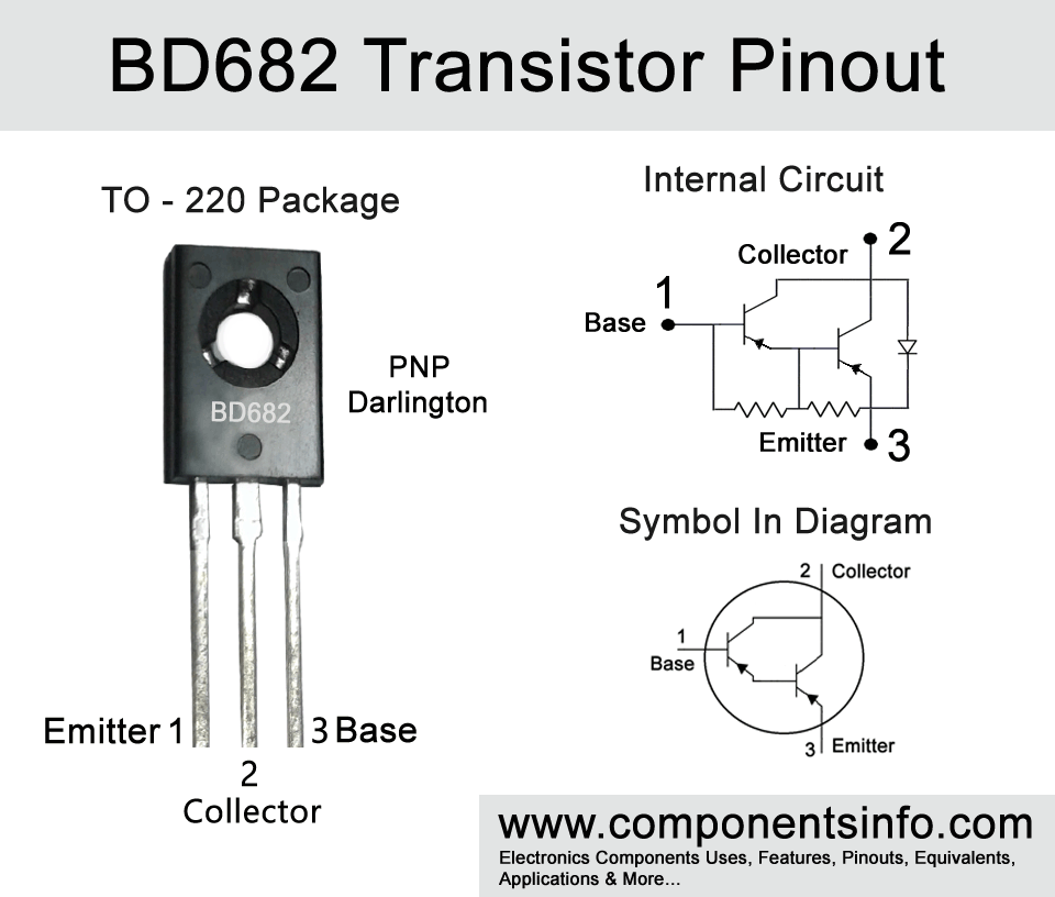
BD682 Transistor Pinout, Equivalent, Applications, Features and Other Information
This post explains BD682 Transistor pinout, equivalent, applications, features and other details such as where and how to use it, safe operating guidelines etc.
Absolute Maximum Ratings:
- Package Type: TO-126
- Transistor Type: PNP Darlington
- Max Collector Current(IC): -4A
- Max Collector-Emitter Voltage (VCEO): -100V
- Max Collector-Base Voltage (VCBO): -100V
- Max Emitter-Base Voltage (VEBO): -5V
- Max Collector Power Dissipation (Pc): 40 Watt
- Minimum DC Current Gain (hFE): 750
- Max Storage & Operating temperature: -65 to +150 Centigrade
NPN Complementary:
NPN Complementary of BD682 is BD681
Replacement and Equivalent:
MJE700, MJE702, MJE703, BD682G
BD682 Transistor Explained / Description:
BD682 is a PNP medium power darlington transistor which means it contains two transistor inside connected in a way which increased the gain to great extent. The transistor can drive load of upto 4A with load voltage of upto -100V. The transistor is available in TO-126 package and designed to use in switching and general purpose amplifier applications.
BD682 is the transistor of BD6xx series which also contains other transistors such as BD678, BD678A, BD680, BD680A and BD682.
Looking at the absolute maximum ratings of the transistor the maximum collector current is -4A, collector-base voltage of the transistor is -100V, maximum collector-emitter voltage is also -100V, max emitter-base voltage is -5V, max base current is -100mA and total device dissipation is 40W.
Where We Can Use it & How to Use:
BD682 is designed to be used in switching and amplifier applications but it can also be used in variety of other applications.
For using the transistor first it is important to know the pinout of the transistor. After knowing the pinout connect the transistor’s base with the signal you want to amplify or with the signal you want to control a load. If you want to use it as a switch to drive load, connect its Emitter with the positive supply of the circuit and it’s Collector with the positive connection of the load and the negative connection of the load will be connected with the ground or negative supply of the circuit. In case of using it as an amplifier the output from the collector will be used as an amplified signal. But it is important to know that for making a good amplifier you have to use some passive components.
Applications:
Motor Control
Audio Amplifiers
Switching Circuits
Pulse Generator
LED Drivers
DC to DC Converters
Voltage Regulation
Battery Operated Applications
Voltage inverters
Power Supplies
Safe Operating Guidelines:
Below are some safe operating guidelines for this transistor.
- For getting long term and stable performance it is important not drive the transistor to its absolute maximum ratings and use it atleast 20% below from its absolute max ratings.
- So the max collector current is -4A but we will not drive load of more than -3.2A.
- The max collector to emitter voltage is -100V therefore the load requirements should be under -80V.
- And the storage and operating temperature of the transistor should be above -55°C and below 150°C.
Datasheet:
To download the datasheet just copy and paste the below link in your browser.
https://datasheetspdf.com/pdf-down/B/D/6/BD682_FairchildSemiconductor.pdf