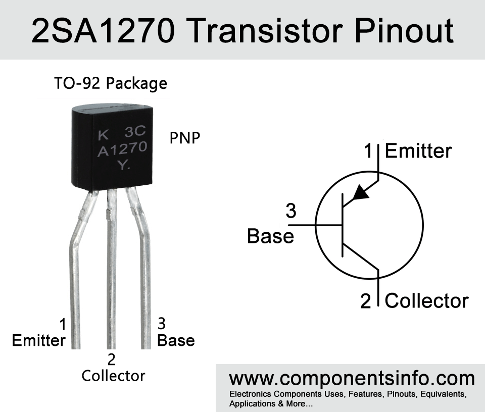
A1270 Transistor Pinout, Equivalent, Uses, Features, Applications and Other Important Info
In this article, we are going explore A1270 transistor pinout, equivalent, uses, features applications, and other important info about this transistor.
Features / Technical Specifications
- Package Type: TO-92
- Transistor Type: PNP
- Max Collector Current (IC): -500mA
- Max Collector-Emitter Voltage (VCE): -30V
- Max Collector-Base Voltage (VCB): -30V
- Max Emitter-Base Voltage (VBE): –5V
- Collector Power Dissipation (Ptot): 500 mW
- DC Current Gain (hFE): 25 to 240
- Max Storage, Operating & Junction temperature range: -55 to +150 Centigrade
Replacement and Equivalent
KSA708C, 2SA1283, BC636, 2SA1526 KSA931, BC636, 2SA1527, BC636, 2SA993, 2SA200, 2SA1522
A1270 Transistor Explained / Description
A1270 or the full part number 2SA1270 is a TO-92 package PNP transistor designed to use in applications such as low power amplifiers, low frequency amplifiers general drivers stage amplifiers and various type of general purpose switching applications.
Moreover, there are many features packed in this small TO-92 package such as collector current of -500mA so it can handle many loads such as relays, LEDs, power transistors etc., collector power dissipation is 500mW, collector power dissipation is the limit of power the transistor’s collector can handle without getting overheated, it has low collector-emitter saturation voltage which means it is power efficient and save from the power loses during operation, transition frequency of upto 200MHz makes the transistor capable to work on higher frequencies required in various applications.
Now looking at the maximum ratings of the transistor the max collector-base voltage is -35V, max collector-emitter voltage is -30V, the emitter-base voltage is -5V, max collector current is -500mA and max collector power dissipation is 500mW.
The transistor comes in two difference version according to its hFE and can be determined with the help of the alphabet written after the part number. If that alphabet is “O” then that transistor gain will be 70-140 and if that alphabet is “Y” then the gain is of that transistor will be 120 to 240.
Where We Can Use it & How to Use
According to its electrical characteristics this transistor can be used in any general purpose application that falls under its capabilities or ratings. Using procedure is the same as we use other general purpose BJT transistors.
Applications
Audio amplifier circuits
RF circuits around 200MHz
Switching circuits
And variety of other general purpose applications.
Safe Operating Guidelines
Before using a transistor it is essential to read the absolute maximum ratings of the transistor and stay 20% below from its absolute maximum ratings in all conditions. So the maximum collector current is -500mA therefore the driven load should be under -400mA, maximum power dissipation should be under 500mW and always store or operate the transistor above -55°C and below +150°C.
Datasheet
To Download the datasheet just copy and paste the below link in your browser.
https://z3d9b7u8.stackpathcdn.com/pdf-down/2/S/A/2SA1270_KEC.pdf