2SC5763 Transistor Pinout, Equivalents, Features, Application, Specs and More
2SC5763 is an NPN BJT (Bipolar Junction Transistor) available in TO-220 package. It is a power transistor and has some good features. It is designed for switching regulators but can also be used in other applications. In this post we will discuss 2SC5763 transistor pinout, features, equivalents, applications, specifications and other details.
Understanding the 2SC5763 Transistor:
2SC5763 is an NPN transistor which means it internally contains three semiconductor layers which are N-type/P-type/N-type. The internal structure of the transistor is as follows:
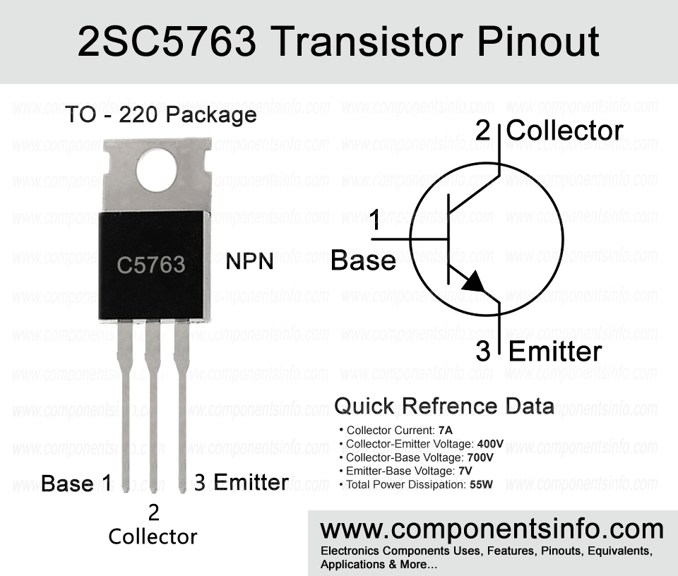
As you can see in the pinout image below the transistor has three pins which are Emitter, Base and Collector. The Emitter is an N-type region and it is heavily doped and emits electrons or in easy words we can say that it has many electrons that are ready at any moment. The base pin has a thin P-type region from which we can control the movement of electrons or how much electrons should flow from the Emitter N-type to the Collector N-type. The last pin is the Collector pin which is also a N-type but has different work, the Collector pin has moderately doped region means it collects electrons.
Now looking at the features of the transistor the transistor has high collector-emitter break down voltage, wide safe operating area, good collector current, fast switching speed, transition frequency is 17MHz and DC current gain is from 20 to 50. The transistor is available in two different versions according to its DC current gain and can be determined with the help of the alphabet written after the part number. The letter “M” shows that the transistor has the DC current gain of 20 to 40 and the letter “N” shows that the transistor has the DC current gain of 30 to 50.
Pin Configuration:
The pin configuration of the transistor are as follows:
Pin1 is the Base pin: As we have already discussed above the base pin is the control pin through which we can control the flow of current from Emitter to Collector.
Pin2 is the Collector pin: In an NPN transistor the current moves from Collector to Emitter so the current first enters in the load the is connected between the positive rail and the collector and then enters into the transistor.
Pin3 is the Emitter pin: The Emitter pin is the from where the current flows to the outside and moves to the negative rail of the circuit making the circuit complete if the required base current is available.
Here are the features and specifications of the transistor:
- Package Type: TO-220
- Transistor Type: NPN
- Max Collector Current(IC): 7A
- Peak Collector Current(ICM): 14A:
- Max Collector-Emitter Voltage (VCEO): 400V
- Max Collector-Base Voltage (VCBO): 700V
- Max Emitter-Base Voltage (VEBO): -5V
- Continuous Base Current(IB):
- Max Collector Power Dissipation (Pc): 55 Watt
- Minimum DC Current Gain (hFE): 20 to 50
- Max Storage & Operating temperature: -55 to +150 Centigrade
Replacement & Equivalent
2sc2335, KSC2335, BUL48, NTE379, MJE5742, BUT12, BUL89, BUL67, BUD47.
Advantages & Disadvantages Of Using 2SC5763:
Here we are pointing advantages and disadvantages of choosing 2SC5763 for your circuit or applications.
Advantages:
Fast Switching Speed: The transistor’s turn on time is 0.5us, storage time is 2.5us and fall time is 0.25us which makes this transistor’s switching speed faster than the other normal transistors.
High Breakdown Voltages: It has high breakdown voltages such as the collector-emitter voltage is 700V and the collector-base voltage is 400V.
Upto 7A Collector Current Capacity: The collector current of 7A is an ideal current to handle medium current load, the peak collector current is 14A.
Wide Safe Operating Area (SOA): This is another advantage of this transistor also mentioned in the datasheet which means it can work safely in different current and voltage conditions which increases its reliability.
Disadvantages:
Low Transition Frequency: The transition frequency of the transistor is only 17MHz which is relatively low as compare to other switching transistors that has higher transition frequencies.
High Saturation Voltage: The transistor is having high saturation voltage which result in some power loss during operation. The collector-emitter saturation voltage is 0.8V and base-emitter saturation voltage is upto 1.5V. These values are higher and you can find low saturation values transistors easily if you are building an application where power loss is a main concern.
Low DC Current Gain: The DC current gain values of the transistor is low, therefore we will need higher drive current at base for switching large current loads.
2SC5763 Applications:
This transistor is specially designed for switching regulator applications but due to its good specifications it can also be used in variety of other circuit such as:
Switching regulators
Motor Drivers
Switch More Power Supplies
DC to DC Converters
Audio Amplifiers (But not ideal to use in audio amplifier)
Conclusion:
The 2SC5763 is a good medium to high power NPN bipolar junction transistor designed to be used in switching regulators. But its good specifications makes it ideal to use in variety of other applications such as DC to DC converters, motor drivers, SMPS etc.
The transistor offers some good features such as high break down voltage, fast switching speed, up to 7A continuous current and 14A peak current which makes it ideal to be used in variety of medium power to high power electronics applications.
While the transistor offers some good features it also has few limitations, such as low transition frequency, high saturation voltage and low DC current gain.
Overall, it’s a good and reliable transistor for fast switching and other applications mentioned above. So if you are looking for a medium to high power transistor for fast switching and other general purpose applications 2SC5763 is good to go.
Datasheet:
To download the datasheet just copy and paste the below link in your browser.
https://www.alldatasheet.com/datasheet-pdf/view/39149/SANYO/2SC5763.html