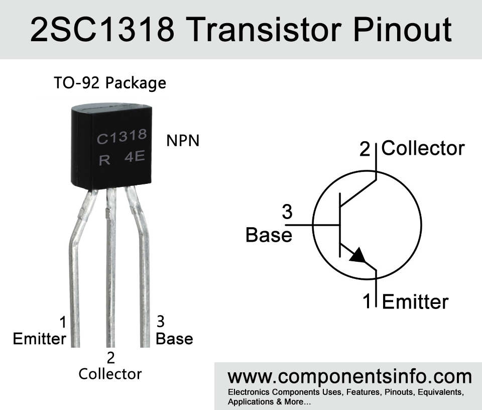
2SC1318 Transistor Pinout, Equivalent, Features, Applications and Other Information
2SC1318 is a TO-92 package NPN silicon transistor designed to be used in audio amplification circuit stages. In this post we are going to discuss 2SC1318 transistor pinout, equivalent, features, applications and other info.
Absolute Maximum Ratings:
- Package Type: TO-92
- Transistor Type: NPN
- Max Collector Current(IC): 500mA
- Max Collector-Emitter Voltage (VCEO): 50V
- Max Collector-Base Voltage (VCBO): 60V
- Max Emitter-Base Voltage (VEBO): 7V
- Max Collector Power Dissipation (PC): 625mW
- Max Transition Frequency (fT): 200 MHz (TYP)
- Minimum & Maximum DC Current Gain (hFE): 85 – 340
- Max Storage & Operating temperature Should Be: -55 to +150 Centigrade
PNP Complementary:
The PNP complimentary of 2SC1318 is 2SA720
Replacement and Equivalent:
2SD438, 2SC3940A, 2SC3923, 2SC3921, 2SC3919, 2SC3917, 2SC4145, 2SD1930, ECG382, NTE382, TIPK111.
2SC1318 Transistor Explained / Description:
2SC1318 is a NPN transistor available in TO-92 package. The transistor designed for low frequency power amplification means it can be used to amplify audio and other similar signals. Another application for which this transistor is built to use in is driver amplification, this means an application used between the source and the power amplifier in which the signal is amplified by a driver circuit or stage to make the signal to the level at which it is amplified by the power amplifier.
Looking at the absolute maximum ratings of the transistor the maximum collector current is 500mA, max collector to emitter voltage is 50V, max emitter to base voltage is 7V, max collector to base voltage is 60V and max collector power dissipation is 625mW.
The transistor is available in three different DC current gain version and each one can be determined with the help of the alphabet written after the part number so if that alphabet is “Q” then its gain will be 85 to 170, if “R” then its gain will be 120 to 240 and if “S” then 170 to 340.
Where We Can Use it & How to Use:
This transistor is mainly designed for driver amplification & low frequency power amplification applications but it is not limited to these applications and can also be used in wide variety of other applications. To use this transistor first of all confirm its pin configuration by looking at the pinout image above, then connect the “Base” with the signal source, connect the “Emitter” pin with the negative supply and connect the “Collector” with one side/wire of the load and other side/wire of the load will be connected with the positive line of the circuit.
Applications:
Audio Amplifiers
Switching Circuits
Battery Chargers
Solar Circuits
Variety of General Purpose Applications
Safe Operating Guidelines:
For good long term performance it is important to follow the safe operating guidelines to operate the transistor. First of all do not drive the transistor to its absolute maximum ratings and always stay at least 20% below from its absolute maximum ratings. So the maximum collector of the transistor is 500mA therefore do not drive load of more than 400mA. The maximum collector to emitter voltage is 50V so do not drive load of more than 40V and always store of operate the transistor at temperature above -55°C to 150°C.
Datasheet:
To download the datasheet just copy and paste the below link in your browser.
https://z3d9b7u8.stackpathcdn.com/pdf-down/2/S/C/2SC1318_PanasonicSemiconductor.pdf