2N5416 Transistor Pinout, Equivalent, Features, Applications and Other Useful Information
2N5416 is a high voltage metal can transistor available in TO-39 package. The transistor has many features and can be used in wide variety of applications. In this post we are going to discuss 2N5416 transistor pinout, equivalent, features, applications and other useful information about this device.
Features / Technical Specifications
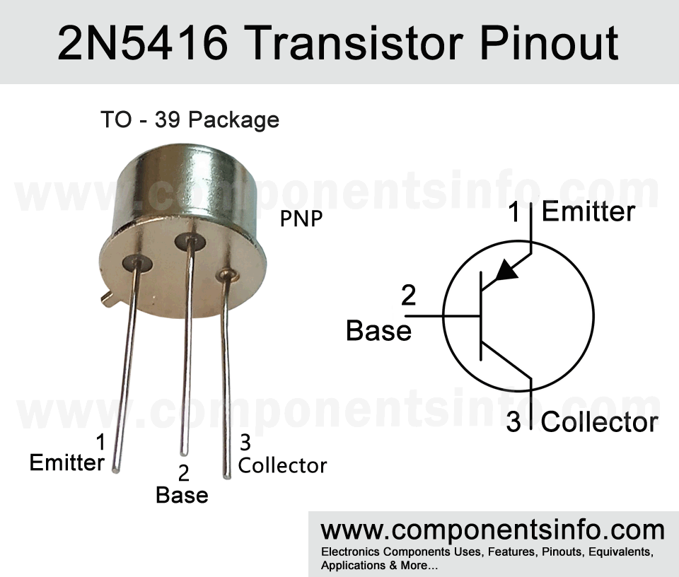
- Package Type: TO-39
- Transistor Type: PNP
- Max Collector Current(IC): –1000mA Or -1A
- Max Collector-Emitter Voltage (VCE): –300V
- Max Collector-Base Voltage (VCB):-200V
- Max Emitter-Base Voltage (VEBO): -6V
- Max Collector Dissipation (Pc): 10 Watt
- Max Transition Frequency (fT): 15 MHz
- Max Base Current (IB): -0.5A
- Minimum & Maximum DC Current Gain (hFE): 30 to 120
- Max Storage & Operating temperature Should Be: -65 to +200 Centigrade
Replacement and Equivalent
2N5416S, MP001173 and its low voltage equivalent 2N5416
2N5416 Transistor Explained / Description
Previously we have discussed 2N5415 transistor, 2N5416 is also the transistor of same series. But it is a more preferred transistor if you want to use in for higher voltages. Like 2N5415, 2N5416 also comes in same metal package TO-39. But when it comes it its absolute maximum ratings and its electrical characteristics they have slight differences which are mentioned below:
Collector to Emitter Voltage:
The collector to emitter voltage of 2N5416 transistor is -200V while the 2N5416 collector to emitter voltage is -300V.
Collector to Base Voltage:
Collector to base voltage of 2N5415 is -200V and 2N5416 is -350V.
Collector to Emitter Sustaining Voltage:
The collector to emitter sustaining voltage of 2N5415 is -200V and 2N5416 is -300V.
DC Current Gain:
The DC current gain also has slightly different but it will not make a big effect. The 2N5415 DC current gain is 30 to 150 while the 2N5416 DC current gain is 30 to 150.
Features
The main feature of 2N5416 transistor is its high collector to emitter voltage which is upto -300V. The high collector to emitter voltage ensures the transistor capability to drive high voltage loads.
Another good feature of the transistor is its high storage and junction temperature that is about -65 °C to 200 °C which makes it ideal and reliable to use in high temperature environment and makes it fail proof.
The transistor also has the transition frequency of 15MHz, the high transition frequency shows the transistor’s capability of speed switching. Which means that the transistor is capable for many high speed switching applications. Moreover the transition frequency of 15MHz also makes it capable to amplify signals of higher frequency when used in an audio amplifier and also in RF applications under 15MHz.
Looking at the specs of the transistor the collector to emitter voltage is -300V, collector to base voltage is -350V, collector current is -1A, base current is -0.5A, emitter to base voltage is -6A, total device dissipation is 10W and minimum and maximum storage and operating temperature is -65°C and +200 °C.
Where We Can Use it & How to Use
This transistor is suitable to use in series regulators, switching circuits, inverters that has high voltage but low current and wide variety of many commercial and industrial uses.
Applications
Audio Amplifiers
Switching Circuits
Oscillators
Power Amplifiers
Motor Control Circuits
Pulse Generators
Voltage Regulators
RF Circuits
Inverters
Power Supplies
High Voltage Power Supply
Inverters
Safe Operating Guidelines:
Before using a transistor in your electronic design or circuits it is important to know the safe operate guidelines for example how much max voltage and current it is capable to handle in safe limit and what minimum and maximum temperature it can handle. The absolute maximum ratings doesn’t mean you can drive the transistor on these limits, the absolute maximum ratings are only to show the max limits of the transistor and driving any transistor on its absolute maximum ratings is also not recommended by the manufacturer so we always suggest to use the transistor 20% below from its absolute maximum ratings. So same applies to this transistor also.
- The max collector to emitter voltage is -300V so according to the 20% rule the driven load should be atleast -240V.
- The max collector current is -1000mA therefore do not drive load of more than 800mA.
- A proper heatsink will be required with the transistor.
- The storage and operating temperature should be between -65°C and +200 °C.
Datasheet
To Download the datasheet just copy and paste the below link into your browser.
https://z3d9b7u8.stackpathcdn.com/pdf-down/2/N/5/2N5416_STMicroelectronics.pdf