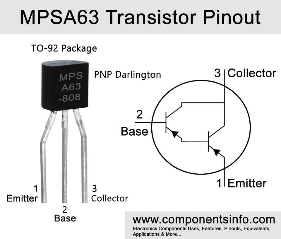
MPSA63 Transistor Pinout, Features, Applications, Equivalents, Specs and More
If you are looking for a PNP darlington transistor with TO-92 package and an acceptable gain value then MPSA63 can be good transistor to use in your design or circuit. In this post we will discuss MPSA63 transistor pinout, features, applications, equivalents, specs and details about where and how to use this transistor.
Absolute Maximum Ratings:
- Package Type: TO-92
- Transistor Type: PNP Darlington
- Max Collector Current(IC): -500mA
- Max Collector-Emitter Voltage (VCE): -30V
- Max Collector-Base Voltage (VCB): -30V
- Max Emitter-Base Voltage (VEBO): -10V
- Max Collector Dissipation (Pc): 625 miliWatt
- Max Transition Frequency (fT): 125 MHz
- Minimum & Maximum DC Current Gain (hFE): 5000
- Max Storage & Operating temperature Should Be: -55 to +150 Centigrade
PNP Complementary:
PNP Complementary of MPSA63 is MPSA13.
Replacement and Equivalent
MPSA65, MPSA64
MPSA63 Transistor Explained / Description
A Darlington transistor is a good choice for applications where we require large DC current gain. The reason behind this large current gain is the pair of transistors connected in such a way that multiplies the DC current gain of the transistor to a great extent. MPSA63 is also a PNP darlington transistor available in TO-92 package and some manufacturers also make it in other small packages like SOT-23 and SOT-223. It is the transistor of a series which is from MPSA62 to MPSA64. The transistor is designed to be used in a variety of general purpose applications and has quite good specifications.
Looking at the absolute maximum ratings of the transistor, the maximum continuous collector current of the transistor is -500mA but some manufacturers also manufacture it in more than -500mA continuous collector current. The maximum collector to emitter voltage is -30V, max collector to base voltage is also -30V, the max emitter to base voltage is -10V and max collector dissipation is 625miliwatt.
Some electrical characteristics of the transistor are transition frequency of 125 MHz, DC current gain is upto 5000, collector-emitter saturation voltage is -1.5V and base-emitter ON voltage is -2.0.
Where & How to Use
MPSA63 can be used in places or designs that require the amplification of low gain signals to very high gain. For example amplification of audio or its preamplification, signal amplification, etc. Moreover, it can also be used as a high gain switch or where you want to control the load with a very low current.
The using procedure of the transistor is the same as we use any normal BJT transistor such as 2N3904 or others. The emitter should be connected to the negative supply, the base should be connected to the input signal through a resistor and the collector should be connected to the negative terminal of the load and the positive terminal of the load should be connected to the positive supply.
Applications
Audio Preamplifiers
Audio Amplifier Stages
Sensor Circuits
Signal Conditioning
Switching Loads under 0.5A
Driver Circuits
Safe Operating Guidelines
To get long term and good performance from any transistor it is important to know the safe operating guidelines which include not operating the transistor to its absolute max ratings and always staying 20% below these absolute maximum ratings. So according to this 20% below operating rule the maximum collector to emitter voltage is -30 so do not drive a load of more than -24V, max continuous collector is -500mA therefore do not drive a load of more than 400mA. The total device dissipation should be under 625mW and the storage and operating temperature should not be between -55 °C to +150°C.
Datasheet
To Download the datasheet just copy and paste the below link in your browser.
https://z3d9b7u8.stackpathcdn.com/pdf-down/M/P/S/MPSA62_ONSemiconductor.pdf