J174 JFET Pinout, Equivalent, Features, Applications and Other Useful Info
J174 is a reliable P Channel JFET available in TO-92 and SOT-23 packages. It is a versatile transistor and can be used in variety of applications. This post covers J174 JFET pinout, equivalent, features, applications and other useful info about this transistor.
Features / Technical Specifications:
- Package Type: TO-92 & SOT-23
- Transistor Type: P Channel JFET
- Maximum Drain to Gate Voltage: -30V
- Max Gate to Source Voltage: 30V
- Gate to Source Cutoff Voltage: 5.0 to 10V
- Max FWD Gate Current: 50mA
- Zero to Gate Voltage Drain Current : -20mA to -100mA
- Maximum Device Dissipation: 350mW
- Drain to Source On Resistance: 85Ω
- Max Storage & Operating temperature Should Be: -55°C to +150 °C
Replacement and Equivalent:
PMBFJ174
J174 Transistors Explained / Description:
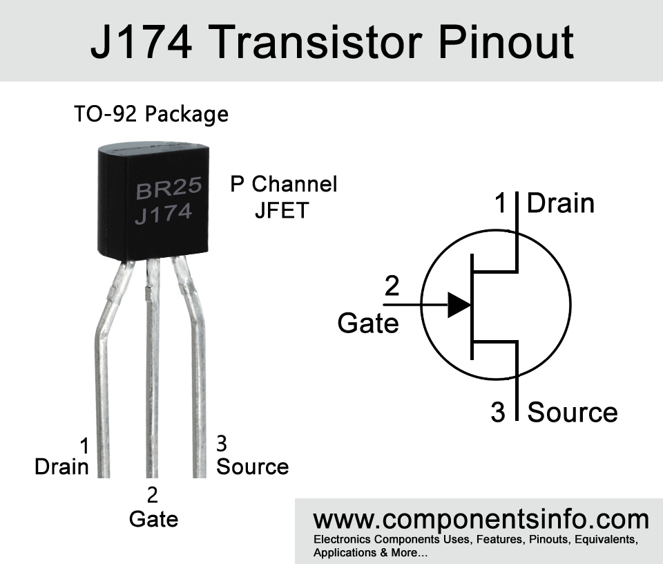
J174 is a P Channel Junction Field Effect Transistor or JFET available in TO-92 and SOT-23 packages. Looking at the pin diagram of the transistor the first pin of the transistor is “Source” second is “Gate” and the third is “Drain”. The technical specs of the transistor are maximum drain to gate voltage is -30V, max gate to source voltage is 30V, gate to source cutoff voltage is 5.0 to 10V, max FWD gate current is 50mA, zero to gate voltage drain current is -20mA to 100mA, max device dissipation is 350mW and max drain to source on resistance is 85 Ohms.
J174 is actually a transistor of J17X series in this series there are also other transistors which are J175, j176 and J177. The electrical characteristics of the J174 are almost the same as the other transistors in the series, but there are some differences which are their “Gate to Source Cutoff Voltage”, “Drain Current”, “Drain to Source On-resistance”, Static Characteristics such as switching times.
The transistor is designed to use in sample and hold circuits. Sample and hold circuit is an electronic application that holds a sample of an analog signal till the next signal is received. These types of circuits are used in applications where accuracy is required for example in communication devices (for converting analog signal to digital), medical devices, scientific instruments, automotive systems, robotics etc.
Another application of the transistor is chopper stabilized amplifier. A chopper stabilized amplifier circuit reduces noise and drift in an electrical signal, first, it cuts a low level electrical signal into multiple small AC signals and amplifies these small signals separately and after separate amplification, it combines all these amplified signals and again converts it to a DC signal. A chopper stabilized amplifier circuit is also used in equipment that requires accuracy for example medical equipment, measurement equipment etc.
The transistor has many features such as low on-resistance, low error voltage, low leakage, fast switching, better frequency response, low insertion loss, low capacitance, good overall accuracy, etc.
Where We Can Use it & How to Use:
As discussed above it is designed to use in sample and hold circuits, shopper stabilized amplifiers etc. The more detailed list of its applications can be found under the “Applications” heading blow. To use the transistor correctly it is suggested to check all the operating and biasing parameters and conditions in the datasheet.
Applications:
Switching Circuits
Voltage Regulators
Signal Modulation & Demodulation
Sample and Hold
RF Amplifiers
Oscillators
Automotive Applications
Low Level Signal Amplification
Instrumental Amplifier
Low Noise Applications
Safe Operating Guidelines
To safely operate the transistor it is suggested to not drive it to its absolute maximum ratings and always stay at least 20% below from these ratings. Moreover, always store or operate the transistor at temperatures above -55°C and below +150 °C.
Datasheet:
To Download the datasheet just copy and paste the below link in your browser.
https://z3d9b7u8.stackpathcdn.com/pdf-down/J/1/7/J174_FairchildSemiconductor.pdf