BC413 Transistor Pinout, Equivalents, Features, Applications, Advantages, Disadvantages and More
BC413 is a TO-92 package NPN transistor designed to be used in general purpose applications. This post discusses on BC413 transistor pinout, equivalents, features, applications, advantages, disadvantages and more.
Understanding the BC413 Transistor:
As discussed above BC413 is an NPN transistor it is a high gain and low noise transistor with very good transition frequency, as it is an NPN transistor it contains three semiconductor layers inside which are N-type/P-type/N-type.
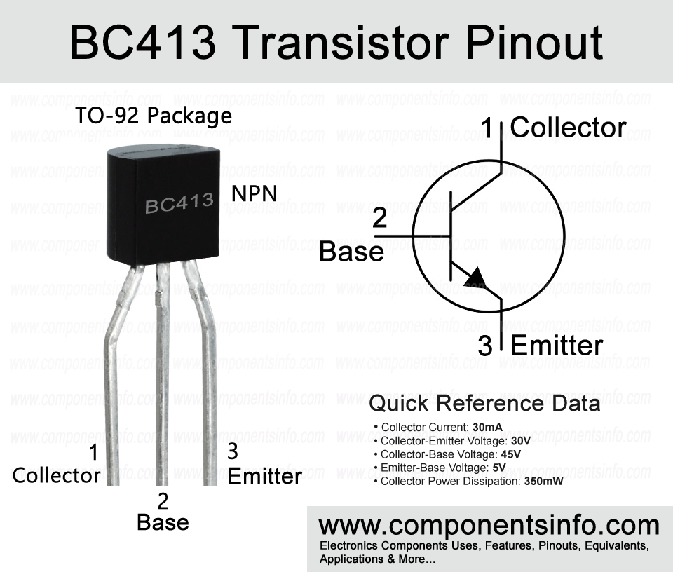
The pinout image below shows the output pins of the transistor which are Emitter, Base and Collector. The Emitter pin is an N-type region and is heavily doped which means that a large number of electrons in this region are ready to flow from the Emitter N-type to Collector N-type. The Base is a thin P-type region which controls the flow of electrons from the Emitter to the Collector. The Collector is also an N-type region but it has a different purpose, it is lightly doped and collect electrons coming from the Emitter N-type region through the Base region and deliver them to the negative rail of the circuit.
The transistor is packed with some good features such as high DC current gain that is from 180 to 800, transition frequency of upto 250MHz, maximum noise figure of 4.0dB and availability of it PNP complimentary.
Pin Configuration:
The pin configuration of the transistor are as follows:
Pin1 is the Collector pin: The Pin1 is the Collector pin, the current first enters in the transistor through this pin and goes to the Emitter through the Base.
Pin2 is the Base pin: The Base is the middle part of the transistor which allows how much current should go to the Emitter. We provide little current to the base pin to control the large flow to the Emitter from Collector.
Pin3 is the Emitter pin: Finally Emitter pin is the last pin the current that enters from the collector pin goes through the Base to the Emitter pin but as mentioned before it is an amount of current that we have allowed with the help of the Base by giving the base pin an specific amount of current.
Here are the features and specifications of the transistor:
- Package Type: TO-92
- Transistor Type: NPN
- Max Collector Current(IC): 100mA
- Max Collector-Emitter Voltage (VCE): 30V
- Max Collector-Base Voltage (VCB): 45V
- Max Emitter-Base Voltage (VEBO): 5V
- Max Collector Dissipation (Pc): 350mW
- Minimum & Maximum DC Current Gain (hFE): 180 To 800
- Max Storage & Operating temperature: -55 to +150 Centigrade
Replacement & Equivalent
BC547, NTE2341, ECG2341, C1815, BC183, BC414C, BC184, BC414C, BC237, 2SD1659, BC548, 2SD779, 2SD2213, 2SD2120, BC549, 2SD1930, 2SD1853, 2SD1779, 2SD1660, 2SC4696, 2SC3069, BC550.
Advantages & Disadvantages Of Using BC413:
Here we are pointing advantages and disadvantages of choosing 2SC1959 for your circuit or applications.
Advantages:
Good DC Current Gain: The transistor has the DC current gain of from 180 to 800. This feature make it suitable to amplify weak signals. It is also ideal to use in preamplifier circuits. Due to this high current gain capability it can provide more collector current on low base current.
High Transition Frequency: The transition frequency of upto 250MHz make it ideal to use in RF circuits, also makes it suitable for high frequency amplification.
Small Package: The small TO-92 package is an ideal transistor package for portable devices because it requires low space on PCB.
Good DC Current Gain: The DC current gain of 70 to 400 ensures good amplification and the transistor requires less base current results in its performance in both amplification and switching circuits.
Low Power Consumption: The power dissipation is only 350mW, this low power consumption which it ideal for battery operated circuits and also it generates less heat.
Low Noise Device: The low noise capability of upto 4dB results in low noise amplification of audio and other signals. It is good for the amplification of low gain signals because it removes distortion from the signal during amplification.
Disadvantages:
Low Voltage: The maximum collector-emitter voltage (VCEO) is 30V which is relatively low voltage. Therefore the transistor cannot be use in medium and high voltage circuits.
Low Power Handling: The power handling capability of the transistor is very low due to which you cannot use it for high power amplification and also there is a risk of overload damaging.
Low Collector Current: The collector current is only 100mA which low. This low current limits the transistor for only low current loads. For driving higher current loads you have to selector another high current transistor.
Not Suitable for Switching Higher Loads: The collector current of 100mA limits the transistor in driving higher loads than 100mW. For driving higher loads you have to look collector current is only 500mA due to which you can only drive small loads. If you want to drive more loads or higher loads than 500mA you have to look for another transistor.
BC413 Applications:
Audio Amplifiers (Low Power Type)
Audio Preamplifiers
Low Noise Audio Amplification
RF Applications
Low Signal Amplification
Many General Purpose Applications
Conclusion:
The BC413 is a small signal NPN transistor that can be used in many low power applications. The transistor has some good features and capabilities such as high transition frequency, low noise and high current gain which makes it ideal for RF applications, low noise signal amplification and high gain applications. Although this device is not ideal for high power and high current applications. But if you are looking for a small package transistor with some good specs to use in many different type of applications then BC413 might be a good choice.
Datasheet:
To download the datasheet just copy and paste the below link in your browser.
https://www.alldatasheet.com/datasheet-pdf/view/606708/CDIL/BC413.html