BD649 Transistor Pinout, Features, Applications, Equivalents, Advantages, Disadvantages and More
BD649 is an NPN Darlington transistor of the series, the series also contains 3 more transistor some of which we have also discussed in this website. In this article we will discuss BD649 transistor pinout, features, applications, equivalents, advantages, disadvantages and other details.
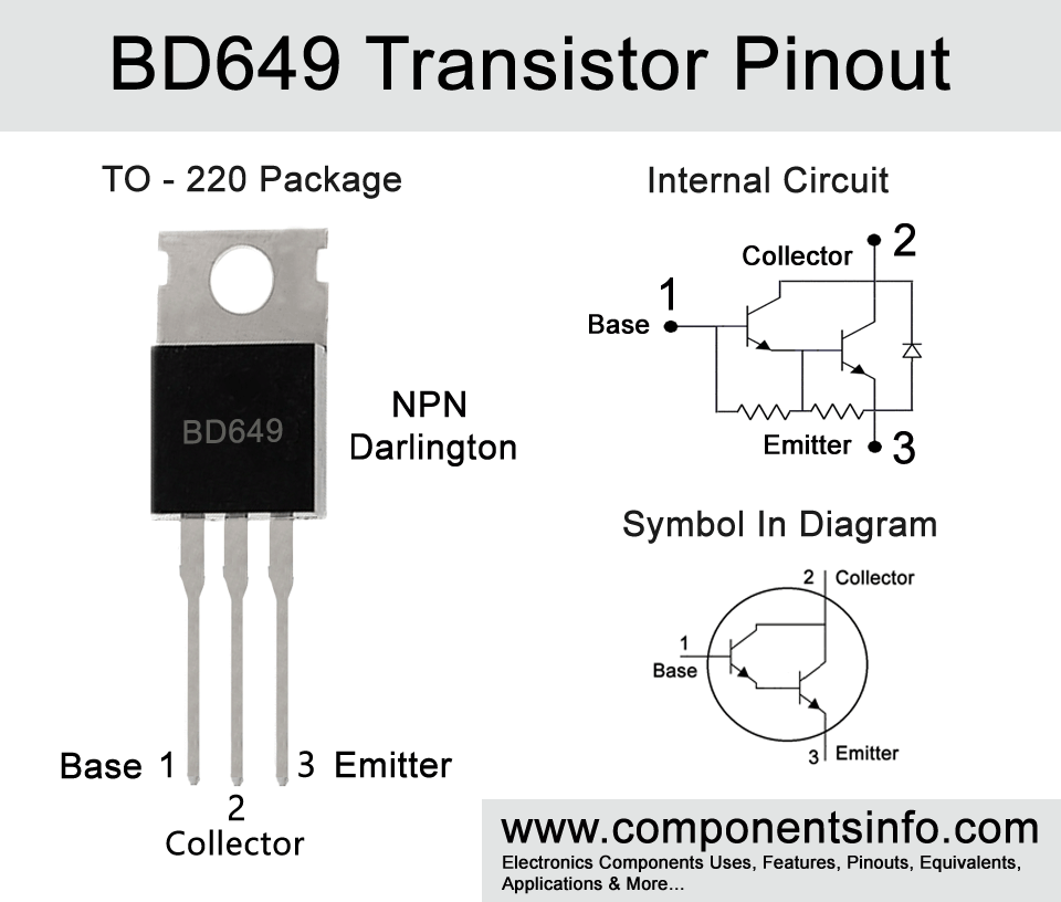
Understanding the BD649 Transistor:
BD649 is an NPN Darlington transistor designed to be used in AF push pull output stages. It is a transistor of a NPN series which also contains other Darlington transistors which are BC643, BD645 and BD647.
A Darlington transistor is actually looks same outside like a normal transistor but internally it contains two transistors inside that connected in special way which is called Darlington. Connecting transistor in this way can increase the gain at the output of the second transistor inside to a great extent.
Each NPN transistor in the Darlington transistor contains three layers which are N-type / P-type / N-type.
Although BD649 is designed to be used in push-pull amplifier circuits but it is not limited to only these applications and can be used in variety of other applications such as output stages of audio power amplifiers, switching circuits, relay circuits, high power LED driver circuits, motor driver circuits etc. the detailed list of its application is mentioned under Applications heading below.
Pin Configuration:
The pin configuration of the transistor are as follows:
Pin1 is the Base pin: The first pin of the transistor is the Base pin, the current flow from collector to emitter through the base pin and can be controlled through this pin.
Pins2 is the Collector pin:
Pin2 is Collector pin the output load of the transistor is connected with the Collector pin.
Pin3 is the Emitter pin:
The third pin Pin3 is the Emitter pin of the transistor. The Emitter pin is connected with the ground. In easy words first current enters through the Collector pin, and then goes to the Emitter through the Base pin.
PNP Complementary:
PNP Complementary of BD649 is BD650
Features and Specifications of the Transistor:
- Package Type: TO-220
- Transistor Type: NPN Darlington
- Max Collector Current(IC): 8A
- Max Collector-Emitter Voltage (VCEO): 100V
- Max Collector-Base Voltage (VCBO): 120V
- Max Emitter-Base Voltage (VEBO): 5V
- Max Collector Power Dissipation (Pc): 62.5mW
- Minimum DC Current Gain (hFE): 750
- Max Storage & Operating temperature: -55 to +150 Centigrade
Replacement & Equivalent
BD643, BD645, BD657
Advantages & Disadvantages of Using 2SC5763:
Here are the advantages and disadvantages of choosing BD649 Darlington transistor for your applications.
Advantages:
High Voltage Handling Capability: It has high VCEO that is upto 100V which makes this transistor suitable for high voltage applications.
A High Gain Transistor: The minimum DC current gain of 750, this high gain of a transistor is beneficial to use in circuits in which you want to drive the load with less base current.
Good Collector Current of Upto 8A): The transistor has an acceptable collector current that is 8A. This 8A collector current is enough to drive lots of small and medium power loads.
High Power Dissipation of 62.5 Watts : The maximum watts this transistor can handle is 62.5. You can also use a proper and suitable heatsink to reduce the overheating risk.
Availability of Complementary Transistor: The complimentary pair of the transistor is also available and it is a big advantage. You can pair BD649 with its complimentary for even better performance.
Low Saturation Voltage: The low saturation voltage helps the transistor to minimum voltage drop in the ON state, this feature improve the efficiency of the transistor.
Disadvantages:
Only 8A Collector Current: The 8A collector current if enough if you want to use this transistor for low and medium power loads. But if you are driving a little higher load than this then this transistor will not work.
Saturation Voltage of 2 to 2.5V: The Darlington transistors has high saturation voltage which makes some power loss and makes the transistor non ideal for portable and battery operated applications.
Slow Switching Speed: Darlington transistors are not very fast in switching due to which it cannot be used in applications that requires fast switching speed.
High VBE : When comparing the Darlington to a normal BJT transistors, the Darlington transistor has high VBE which also makes it non ideal for low voltage circuits.
Applications:
Audio Amplifiers
Relay Drivers
DC Motor Drivers
Battery Chargers
Push-Pull Amplifiers
Power Supply Circuits
Voltage Regulators
Switching Circuits
Conclusion:
BD649 is an NPN Darlington transistor designed to be used in AF push pull output stages but can also be used in wide variety of other applications. The maximum VCEO of the transistor is 100V which makes it ideal to use in high voltage applications. The maximum collector current is 8A which is a good collector current to drive variety of small and medium power loads. The power dissipation of the transistor is 62.5W and there is also a complimentary pair of this transistor that is BD650. But the transistor also have some limitations such as high VBE, low switching speed, only 8A collector current so it can only be used to drive low and medium power loads. But if you want a Darlington that is good for audio frequency push pull output stage or you want to use it for general purpose applications than this transistor will work well.
Datasheet:
To download the datasheet just copy and paste the below link in your browser.
https://www.alldatasheet.com/datasheet-pdf/view/269344/ISC/BD649.html