2SC1959 Transistor Pinout, Features, Equivalent, Uses and Other Details
2SC1959 is a very interesting PNP transistor available in TO-92 package. The transistor is designed to be used in variety of electronics applications. This post explains 2SC1959 transistor pinout, features, equivalents, uses and other details about this transistor.
Understanding the 2SC1959 Transistor:
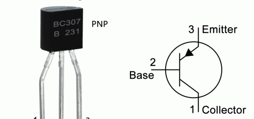
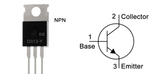
2SC5763 is an NPN transistor which means it internally contains three semiconductor layers which are N-type/P-type/N-type. The internal structure of the transistor is as follows:
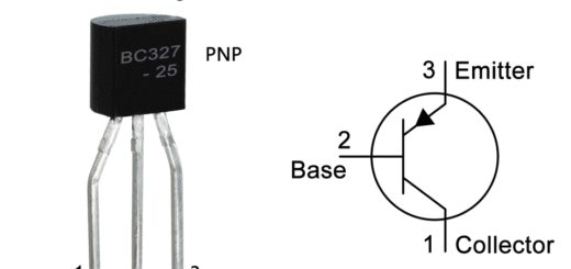
2SC1959 is a PNP transistor which contains three semiconductor layers inside which are P-type/N-type/P-type. Internal structure of the transistor is as follows:
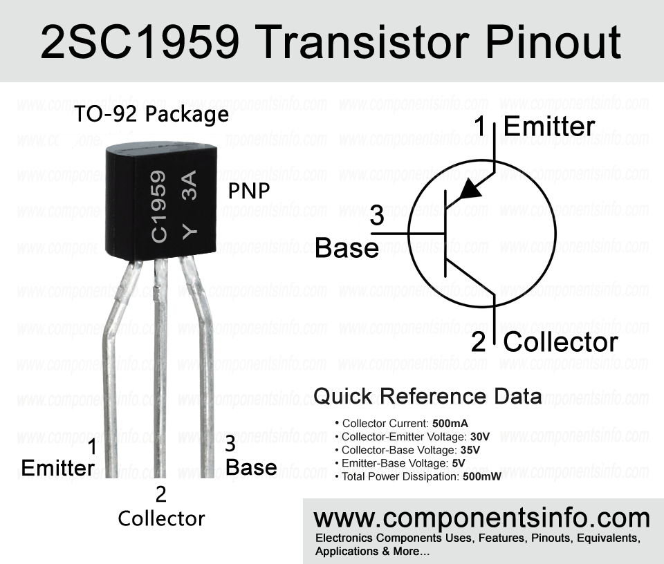
The pinout image below shows three pins of the transistor which are Emitter, Base and Collector. The Emitter pin is a P-type region and it is heavily doped means it has many electrons that are ready to flow any time. The base pin has a thin N-type region through which the flow of electrons from the Emitter (P-type) to Collector (P-type) can be controlled.
The last pin is the Collector pin which is also a P-type but has a different purpose that is it collect electrons.
Now looking at the features of the transistor it has the collector current of up to 500mA which a good collector current for a TO-92 package size transistor, suitable for 1 Watt amplifiers, availability of complimentary transistor, excellent hFE linearity and transition frequency of up to 300MHz.
Pin Configuration:
The pin configuration of the transistor are as follows:
Pin1 is the Emitter pin: The current first enters in the transistor through its Emitter pin and flows to the collector pin but controlled by the base pin.
Pin2 is the Collector pin: The Second pin is Collector the current that enters through the Emitter pin goes to the ground through the collector pin.
Pin3 is the Base pin: The third pin is the base pin that we have already discussed above. We can control the flow of current from Emitter to Collector through the Base pin.
Here are the features and specifications of the transistor:
- Package Type: TO-92
- Transistor Type: PNP
- Max Collector Current(IC): 500mA
- Max Collector-Emitter Voltage (VCEO): 30V
- Max Collector-Base Voltage (VCBO): 35V
- Max Emitter-Base Voltage (VEBO): 5V
- Max Collector Power Dissipation (Pc): 500mW
- Minimum DC Current Gain (hFE): 25 to 400
- Max Storage & Operating temperature: -55 to +150 Centigrade
PNP Complementary:
PNP Complementary of 2SC1959 is 2SA562TM
Replacement & Equivalent
2SC3923, 2SC3921, 2SC3919, 2SC3917, PN2219, PN2222, BC337, BC879, BC637, BC639, 2SD974, 2SD763, SK3849, SK9142, MPS8099, MPS3405, MPS2222, KTN2222, KTC3203, 2SD1835, 2SD1779, 2SD1388, 2SD1207, 2SD1014, 2SC6043, 2SC5335, 2SC4145, 2SC2475, 2SC1959, 2N7052, 2N4401.
Advantages & Disadvantages Of Using 2SC1959:
Here we are pointing advantages and disadvantages of choosing 2SC1959 for your circuit or applications.
Advantages:
Can be Used for Up to 1 Watt Amplifier Applications: The transistor is capable to handle collector current of upto 500mA and power dissipation and make it ideal for applications such as low power amplifiers of up to 1W, amplifier stages, preamplifiers, RF circuits. Moreover the good linearity results in good signal clarity in audio and related applications.
Up to 500mA Collector Current: The current handling capability of up to 500mA makes it suitable for many low power and medium power applications.
High Transition Frequency: The transition frequency of up to 300MHz make this transistor ideal for RF and high frequency applications. Moreover, this features also makes this transistor a good candidate for a switch circuit.
Good DC Current Gain: The DC current gain of 70 to 400 ensures good amplification and the transistor requires less base current results in its performance in both amplification and switching circuits.
Availability of Complimentary Transistor: The availability of its NPN complimentary transistor allows more benefits such as with the combination of both you can build many different types of amplifiers such as class-AB, push-pull, etc.
Disadvantages:
Low Voltage: The maximum VCEO is 30V and VCBO is 35V which is relatively low voltage. Due to these low voltage ratings the transistor cannot be used in many circuits.
Low Power Dissipation: The power dissipation of the transistor is relatively low due to which it cannot handle high loads because low heat dissipation capability makes the device overheat if you have connected the high loads.
Not Suitable for High Power Loads: The collector current is only 500mA due to which you can only drive small loads. If you want to drive more loads or higher loads than 500mA you have to look for another transistor.
2SC1959 Applications:
Audio Amplifiers (Low Power Type)
Different types of Signal Amplifications
RF Applications
Driver Stages
Many other General Purpose Applications
Conclusion:
2SC1959 is a useful transistor that can be used in wide variety of applications. The 500mA of load driving capability, high transition frequency and good DC current gain makes it suitable to use in many audio amplifiers, RF and Switching applications. Moreover you can also use it with its NPN complimentary. On the other hand the low voltage and low heat dissipation makes it unsuitable for high voltage and power applications. But if you are looking for a small signal general purpose transistor then 2SC1959 might be a good choice.
Datasheet:
To download the datasheet just copy and paste the below link in your browser.
https://www.alldatasheet.com/datasheet-pdf/view/30086/TOSHIBA/2SC1959.html


