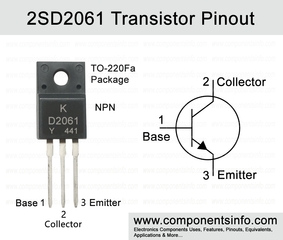
2SD2061 Transistor Pinout, Features, Uses, Equivalent and Other Details
The D2061 full part number 2SD2061 is an NPN power transistor available in TO-220Fa package. In this article, we will discuss about 2SD2061 transistor pinout, features, uses, equivalent and other details about this component.
Absolute Maximum Ratings:
- Package Type: TO-220
- Transistor Type: NPN
- Max Collector Current(IC): 3A
- Max Collector-Emitter Voltage (VCE): 80V
- Max Collector-Base Voltage (VCB): 60V
- Max Emitter-Base Voltage (VEBO): 5V
- Total Power Dissipation (PC): 30 Watts
- Max Transition Frequency (fT): 8 MHz
- Minimum & Maximum DC Current Gain (hFE): 100 – 320
- Max Storage & Operating temperature Should Be: -55 to +150 Centigrade
Replacement and Equivalent:
TIP41D, MJE15028, BDX77, BDT87, BDT85, BDT83, BD955, BD951, BD809, BD801, BD797, BD545A/B/C, BD543A/B/C, BD539, BD535, BD243A/B/C, BD241A/B/C, 2SD823, 2SD313, 2SD2012, 2SD1274, 2SD1266, 2SC4552, 2SC4550, 2SC4007, 2SC3851, 2SC2315, TIP152, TIP150, TIP112, MJF10012, KSC1983,2SD1530, 2SC4554, 2SC4496.
2SD2061 Transistor Explained / Description:
2SD2061 is an NPN power transistor available in TO-220Fa package and designed to be used in low frequency power amp applications. The absolute maximum rating of the transistor are as follows:
Collector-emitter voltage is 60V, collector current is 3A, collector-base voltage is 80V, emitter-base voltage is 5V, collector power dissipation is 30W, junction temperature is 150°C and storage temperature is -55°C to 150°C.
Looking at the electrical characteristics of the transistor the collector-emitter break down voltage is 60V, collector-base breakdown voltage is 80V, collector-emitter saturation voltage is 1V, DC current gain is 100 to 320 and transition frequency is 8MHz.
According to the DC current gain the transistor is available in two different hFE values which can be identified with the help of the alphabet written after the part number. If that alphabet is “E” then the hFE will be 100 to 200 and if that alphabet is “F” then the hFE will be 160 to 320.
How to Use This Transistor:
It is a NPN BJT (Bipolar junction transistor) therefore the using procedure will be same as we use any other BJT by applying signal to its base, connecting its emitter with the ground or negative rail of the circuit and taking amplified signal output from the collector pin in amplifier circuit and driving load with the collector pin in switch circuit. This is a basic guide how this transistor works or can be used in an amplifier and as a switch but to build a proper working circuit you will also require a schematic diagram of the circuit and passive components that are used in that schematic diagram.
Applications:
Audio Amplifier Circuit
Power Amplifiers
Switching Circuit
And Other General Purpose Circuits
Safe Operating Guidelines:
To safely operate the transistor follow these guidelines:
- Do not use it to its absolute maximum ratings and always stay at least 20% below from these ratings.
- Always use a suitable heatsink with the transistor.
- Confirm pin layout before using in your circuit.
- Always store and operate at temperatures above -50°C and below 150°C.
Datasheet:
To download the datasheet just copy and paste the below link in your browser.
https://www.alldatasheet.com/datasheet-pdf/view/440321/ISC/2SD2061.html