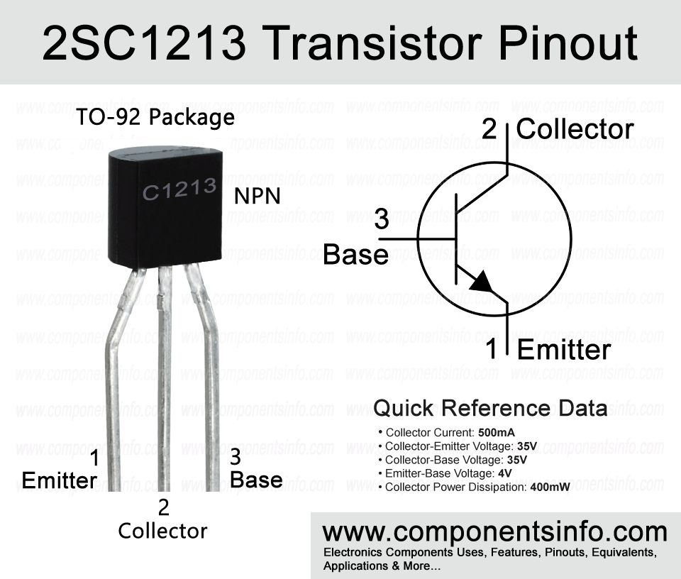
2SC1213 Transistor Pinout, Applications, Equivalent, Features and other Details
2SC1213 or C1213 is an NPN low frequency amplifier transistor available in TO-92 package. Today we will discuss about 2SC1213 transistor pinout, applications, equivalent, features and other details.
Absolute Maximum Ratings:
- Package Type: TO-92
- Transistor Type: NPN
- Max Collector Current(IC): 500mA
- Max Collector-Emitter Voltage (VCE): 35V
- Max Collector-Base Voltage (VCB): 35V
- Max Emitter-Base Voltage (VBE): 4V
- Max Collector Dissipation (Pc): 400 mW
- Minimum & Maximum DC Current Gain (hFE): 60 to 320
- Max Storage, Operating & Junction temperature range: -55 to +150 Centigrade
Replacement & Equivalent
MPS1711, BT2483, BFR41, BDB06, BCX38, BCW91, BC877, BC639, BC637, BC618, BC489, BC487, BC373, 2SD863, 2SD763, 2SD667.
2SC1213 Transistor Explained / Description:
2SC1213 is another interesting transistor packed with some good features such as good collector current, good DC current gain, small package and availability of its NPN complimentary.
The absolute maximum ratings of the transistor are collector-emitter voltage of 35V, collector current is 500mA, collector-base voltage is also 35V, emitter-base voltage is 4V, collector dissipation is 400mW, junction temperature is 150°C and storage temperature is from -55°C to 150°C.
Although the 2SC1841 is designed for low frequency applications, its electrical characteristics make it a versatile transistor that can be used in many different types of applications.
Furthermore, it is available in three different versions based to its DC current gain (hFE) and can be identified with the help of the alphabet written after the part number. The alphabets are “B”, “C” and “D”, “B” means the gain is from 60 to 120, “C” means from 100 to 200 and “D” from 160 to 320.
How to Use This Transistor:
2SC1213 is an NPN bipolar junction transistor; therefore, its usage procedure is same as we use any other BJT. Such as the signal that we want to amplify is fed to the base pin, the negative voltage is provided to the emitter pin and from collector pin we will take the amplified output of our signal and if the transistor is used as a switch then the load will be connected with the collector pin.
The switch circuit is straightforward you just have to connect a current limiting resistor at the base of the transistor and also between the load and the collector pin if your load requires current limiting for example an LED. However, to make a better amplifier circuit you have to use some more passive components for good performance and this requires some previous knowledge of amplifier circuit designs alternatively you can also use a readymade schematics from a book or by searching on internet.
Applications:
Audio amplifiers
Audio amplifier stages
Audio preamplifiers
Switching Circuits
Low Gain Signal Amplification
Safe Operating Guidelines:
To safely operate the transistor always use it at least 20% below from its absolute maximum ratings. Check the transistor’s pin layout before placing in a circuit, the operating temperature should be between 55°C and below +150 °C.
Datasheet:
To download the datasheet just copy and paste the below link in your browser.
https://www.alldatasheet.com/datasheet-pdf/view/62862/HITACHI/2SC1213.html