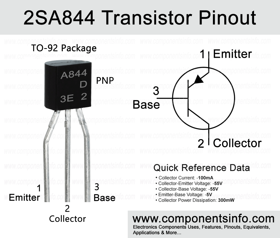
2SA844 Transistor Pinout, Equivalents, Features, Applications and Other Details
A844 is a TO-92 package PNP transistor designed to be used in low frequency amplifier applications. In this post we will explore 2SA844 transistor pinout, equivalents, features, applications and other details of this component.
Absolute Maximum Ratings:
- Package Type: TO-92
- Transistor Type: NPN
- Max Collector Current(IC): –100mA
- Max Collector-Emitter Voltage (VCE): –55V
- Max Collector-Base Voltage (VCB): –55V
- Max Emitter-Base Voltage (VEBO): –5V
- Max Collector Dissipation (Pc): 300 miliWatt
- Max Transition Frequency (fT): 200 MHz
- Minimum & Maximum DC Current Gain (hFE): 160 – 800
- Max Storage & Operating temperature Should Be: -55 to +150 Centigrade
Replacement & Equivalent
2SA844F, BC880, TIPP116, SK3715, BRY56, NTE2342, ECG2342, 2SB1363, 2SB1256, 2SB1212, 2SB1059, 2SA1625, 2SA1193.
2SA844 Transistor Explained / Description:
A844 full part number 2SA844 is a PNP transistor designed to be used in low frequency amplifier applications. The transistor is packed with some of very good features such as good collector-emitter voltage, Dc current gain of 160 to 800 and transition frequency of 200MHz.
Looking at the absolute maximum ratings of the transistor, the collector current is 100mA, collector-emitter voltage is -55V, emitter-base voltage is -5V, collector-base voltage is also -55V, emitter current is 100mA, collector power dissipation is 300mA, junction temperature is 150 °C and storage temperature is from -55 °C to 150°C.
The transistor is available in three different variations according to its DC current gain and can be determined with the alphabetical codes written after their part numbers.
The code “C” means DC current gain of 160 to 320.
The code “D” means DC current gain of 250 to 500.
The code “E” means DC current gain of 400 to 800.
How to Use This Transistor:
It is a BJT (Bipolar Junction Transistor) and it has three pins which are emitter, base and collector. The base pin is where we apply the signal to control the output load (in switch circuit) and to amplify the signal (in amplifier circuit). The emitter pin will be connected with the positive rail of the circuit and the load will be derived with the collector in the switch circuits and the amplified output will also be received at the collector pin in amplifier circuits. But with the procedure we cannot build a proper of effective circuit so we must have to use some discrete components to improve the circuit. To use these discrete components we must require some knowledge and experience of electronics.
Applications:
Audio Preamplifiers
Audio Amplifiers
Sensor Circuits
Signal Amplification
RF Circuits
Darlington Pairs
Switching loads under 1A
And more…
Safe Operating Guidelines:
To safely use the transistor always use the transistor under its absolute maximum ratings and stay at least 20% to 30% from these ratings. Operating and storage temperature should be between -55°C to 150°C.
Datasheet:
To download the datasheet just copy and paste the below link in your browser.
https://www.alldatasheet.com/datasheet-pdf/view/62817/HITACHI/2SA844.html